
Datasheet

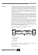
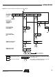
Table Of Contents
- Features
- Description
- Block Diagram
- SFR Mapping
- Pin Configurations
- Oscillators
- Enhanced Features
- Dual Data Pointer Register DPTR
- Expanded RAM (XRAM)
- Reset
- Power Monitor
- Timer 2
- Programmable Counter Array PCA
- Serial I/O Port
- Interrupt System
- Power Management
- Keyboard Interface
- 2-wire Interface (TWI)
- Serial Port Interface (SPI)
- Hardware Watchdog Timer
- ONCE(TM) Mode (ON Chip Emulation)
- Power-off Flag
- EEPROM Data Memory
- Reduced EMI Mode
- Flash Memory
- Electrical Characteristics
- Absolute Maximum Ratings
- DC Parameters
- AC Parameters
- Explanation of the AC Symbols
- External Program Memory Characteristics
- External Program Memory Read Cycle
- External Data Memory Characteristics
- External Data Memory Write Cycle
- External Data Memory Read Cycle
- Serial Port Timing - Shift Register Mode
- Shift Register Timing Waveforms
- External Clock Drive Waveforms
- AC Testing Input/Output Waveforms
- Float Waveforms
- Clock Waveforms
- Ordering Information
- Packaging Information
- Table of Contents
88
AT89C51ID2
4289C–8051–11/05
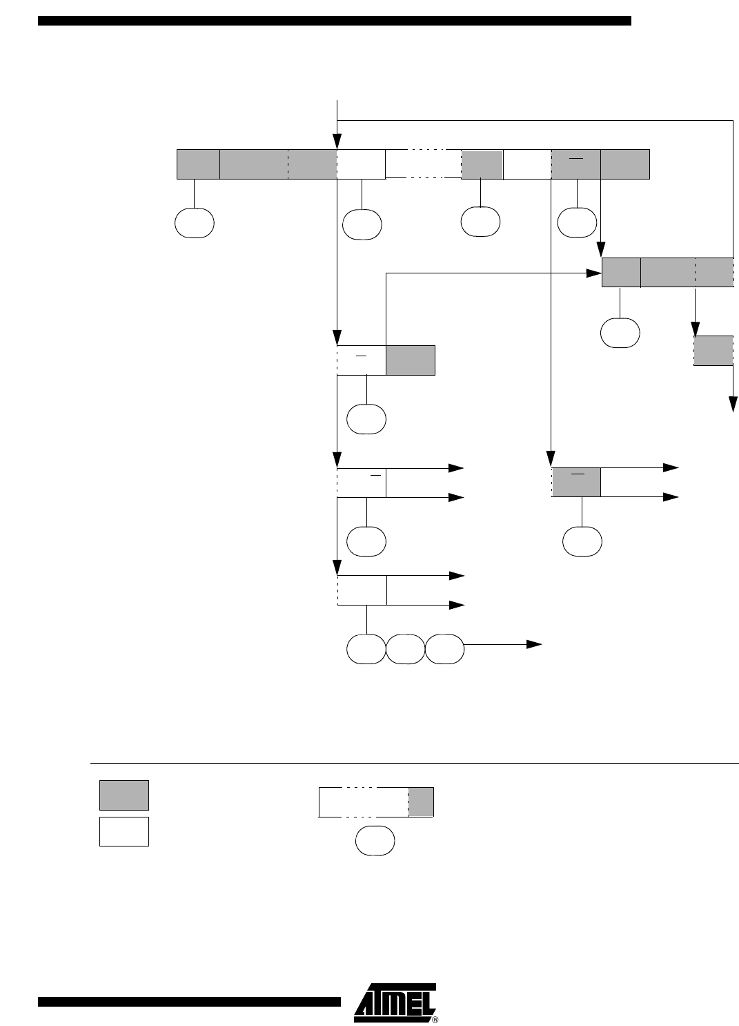
Figure 33. Format and State in the Master Receiver Mode
SSLAR A
Data
08h
40h
58h
SSLAR
AP
W
MT
10h
48h
A or A
continues
38h38h
A
continues
68h
Other master
Other master
78h B0h
To corresponding
states in slave mode
Successfull
transmission
to a slave
receiver
Next transfer
started with a
repeated start
condition
Not acknowledge
received after the
slave address
Arbitration lost and
addressed as slave
A
continues
Other master
n
From master to slave
From slave to master
Any number of data bytes and their associated
acknowledge bits
This number (contained in SSCS) corresponds
to a defined state of the 2-wire bus
A
Data
PA
50h
MR
Arbitration lost in slave
address or acknowledge bit
Data A