
Datasheet
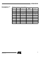
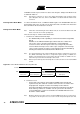
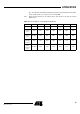
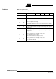
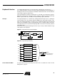
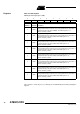
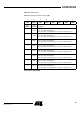
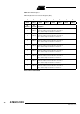
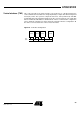
Table Of Contents
- Features
- Description
- Block Diagram
- SFR Mapping
- Pin Configurations
- Oscillators
- Enhanced Features
- Dual Data Pointer Register DPTR
- Expanded RAM (XRAM)
- Reset
- Power Monitor
- Timer 2
- Programmable Counter Array PCA
- Serial I/O Port
- Interrupt System
- Power Management
- Keyboard Interface
- 2-wire Interface (TWI)
- Serial Port Interface (SPI)
- Hardware Watchdog Timer
- ONCE(TM) Mode (ON Chip Emulation)
- Power-off Flag
- EEPROM Data Memory
- Reduced EMI Mode
- Flash Memory
- Electrical Characteristics
- Absolute Maximum Ratings
- DC Parameters
- AC Parameters
- Explanation of the AC Symbols
- External Program Memory Characteristics
- External Program Memory Read Cycle
- External Data Memory Characteristics
- External Data Memory Write Cycle
- External Data Memory Read Cycle
- Serial Port Timing - Shift Register Mode
- Shift Register Timing Waveforms
- External Clock Drive Waveforms
- AC Testing Input/Output Waveforms
- Float Waveforms
- Clock Waveforms
- Ordering Information
- Packaging Information
- Table of Contents

80
AT89C51ID2
4289C–8051–11/05
2-wire Interface (TWI) This section describes the 2-wire interface. The 2-wire bus is a bi-directional 2-wire
serial communication standard. It is designed primarily for simple but efficient integrated
circuit (IC) control. The system is comprised of two lines, SCL (Serial Clock) and SDA
(Serial Data) that carry information between the ICs connected to them. The serial data
transfer is limited to 400 Kbit/s in standard mode. Various communication configuration
can be designed using this bus. Figure 29 shows a typical 2-wire bus configuration. All
the devices connected to the bus can be master and slave.
Figure 29. 2-wire Bus Configuration
SCL
SDA
device2device1 deviceN
device3
...