
Datasheet
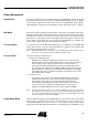
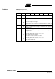
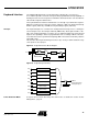
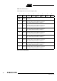
Table Of Contents
- Features
- Description
- Block Diagram
- SFR Mapping
- Pin Configurations
- Oscillators
- Enhanced Features
- Dual Data Pointer Register DPTR
- Expanded RAM (XRAM)
- Reset
- Power Monitor
- Timer 2
- Programmable Counter Array PCA
- Serial I/O Port
- Interrupt System
- Power Management
- Keyboard Interface
- 2-wire Interface (TWI)
- Serial Port Interface (SPI)
- Hardware Watchdog Timer
- ONCE(TM) Mode (ON Chip Emulation)
- Power-off Flag
- EEPROM Data Memory
- Reduced EMI Mode
- Flash Memory
- Electrical Characteristics
- Absolute Maximum Ratings
- DC Parameters
- AC Parameters
- Explanation of the AC Symbols
- External Program Memory Characteristics
- External Program Memory Read Cycle
- External Data Memory Characteristics
- External Data Memory Write Cycle
- External Data Memory Read Cycle
- Serial Port Timing - Shift Register Mode
- Shift Register Timing Waveforms
- External Clock Drive Waveforms
- AC Testing Input/Output Waveforms
- Float Waveforms
- Clock Waveforms
- Ordering Information
- Packaging Information
- Table of Contents
76
AT89C51ID2
4289C–8051–11/05
Keyboard Interface The AT89C51ID2 implements a keyboard interface allowing the connection of a
8 x n matrix keyboard. It is based on 8 inputs with programmable interrupt capability on
both high or low level. These inputs are available as alternate function of P1 and allow to
exit from idle and power down modes.
The keyboard interface interfaces with the C51 core through 3 special function registers:
KBLS, the Keyboard Level Selection register (Table 61), KBE, The Keyboard interrupt
Enable register (Table 60), and KBF, the Keyboard Flag register (Table 59).
Interrupt The keyboard inputs are considered as 8 independent interrupt sources sharing the
same interrupt vector. An interrupt enable bit (KBD in IE1) allows global enable or dis-
able of the keyboard interrupt (see Figure 27). As detailed in Figure 28 each keyboard
input has the capability to detect a programmable level according to KBLS. x bit value.
Level detection is then reported in interrupt flags KBF. x that can be masked by software
using KBE. x bits.
This structure allow keyboard arrangement from 1 by n to 8 by n matrix and allow usage
of P1 inputs for other purpose.
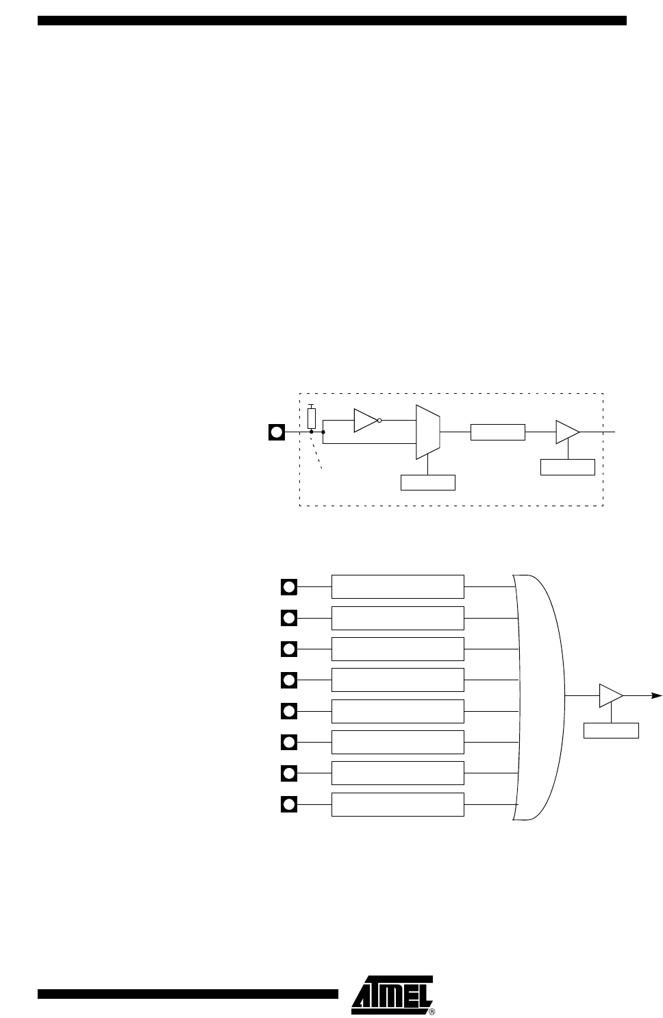
Figure 27. Keyboard Interface Block Diagram
Figure 28. Keyboard Input Circuitry
Power Reduction Mode P1 inputs allow exit from idle and power down modes as detailed in Section “Power
Management”, page 72.
P1:x
KBE. x
KBF. x
KBLS. x
0
1
Vcc
Internal Pullup
P1.0
Keyboard Interface
Interrupt Request
KBD
IE1
Input Circuitry
P1.1 Input Circuitry
P1.2 Input Circuitry
P1.3 Input Circuitry
P1.4 Input Circuitry
P1.5 Input Circuitry
P1.6 Input Circuitry
P1.7 Input Circuitry
KBDIT