
Datasheet
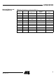
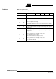
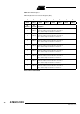
Table Of Contents
- Features
- Description
- Block Diagram
- SFR Mapping
- Pin Configurations
- Oscillators
- Enhanced Features
- Dual Data Pointer Register DPTR
- Expanded RAM (XRAM)
- Reset
- Power Monitor
- Timer 2
- Programmable Counter Array PCA
- Serial I/O Port
- Interrupt System
- Power Management
- Keyboard Interface
- 2-wire Interface (TWI)
- Serial Port Interface (SPI)
- Hardware Watchdog Timer
- ONCE(TM) Mode (ON Chip Emulation)
- Power-off Flag
- EEPROM Data Memory
- Reduced EMI Mode
- Flash Memory
- Electrical Characteristics
- Absolute Maximum Ratings
- DC Parameters
- AC Parameters
- Explanation of the AC Symbols
- External Program Memory Characteristics
- External Program Memory Read Cycle
- External Data Memory Characteristics
- External Data Memory Write Cycle
- External Data Memory Read Cycle
- Serial Port Timing - Shift Register Mode
- Shift Register Timing Waveforms
- External Clock Drive Waveforms
- AC Testing Input/Output Waveforms
- Float Waveforms
- Clock Waveforms
- Ordering Information
- Packaging Information
- Table of Contents

74
AT89C51ID2
4289C–8051–11/05
pins, the instruction immediately following the instruction that activated the Power-Down
mode should not write to a Port pin or to the external RAM.
Note: Exit from power-down by reset redefines all the SFRs, but does not affect the internal
RAM content.
Table 57. Pin Conditions in Special Operating Modes
Mode Port 0 Port 1 Port 2 Port 3 Port 4 ALE PSEN#
Reset Floating High High High High High High
Idle
(internal
code)
Data Data Data Data Data High High
Idle
(external
code)
Floating Data Data Data Data High High
Power-
Down(inter
nal code)
Data Data Data Data Data Low Low
Power-
Down
(external
code)
Floating Data Data Data Data Low Low