
Datasheet
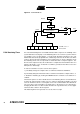
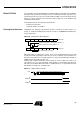
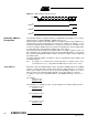
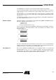
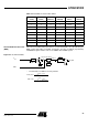
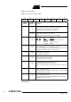
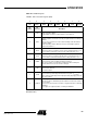
Table Of Contents
- Features
- Description
- Block Diagram
- SFR Mapping
- Pin Configurations
- Oscillators
- Enhanced Features
- Dual Data Pointer Register DPTR
- Expanded RAM (XRAM)
- Reset
- Power Monitor
- Timer 2
- Programmable Counter Array PCA
- Serial I/O Port
- Interrupt System
- Power Management
- Keyboard Interface
- 2-wire Interface (TWI)
- Serial Port Interface (SPI)
- Hardware Watchdog Timer
- ONCE(TM) Mode (ON Chip Emulation)
- Power-off Flag
- EEPROM Data Memory
- Reduced EMI Mode
- Flash Memory
- Electrical Characteristics
- Absolute Maximum Ratings
- DC Parameters
- AC Parameters
- Explanation of the AC Symbols
- External Program Memory Characteristics
- External Program Memory Read Cycle
- External Data Memory Characteristics
- External Data Memory Write Cycle
- External Data Memory Read Cycle
- Serial Port Timing - Shift Register Mode
- Shift Register Timing Waveforms
- External Clock Drive Waveforms
- AC Testing Input/Output Waveforms
- Float Waveforms
- Clock Waveforms
- Ordering Information
- Packaging Information
- Table of Contents
56
AT89C51ID2
4289C–8051–11/05
Table 37. Baud Rate Selection Table UART
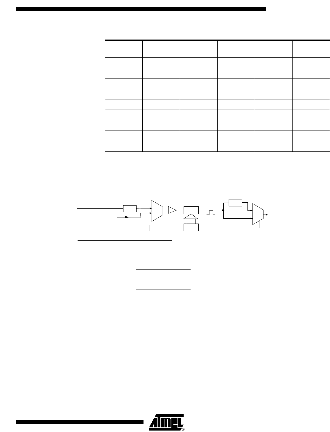
Internal Baud Rate Generator
(BRG)
When the internal Baud Rate Generator is used, the Baud Rates are determined by the
BRG overflow depending on the BRL reload value, the value of SPD bit (Speed Mode)
in BDRCON register and the value of the SMOD1 bit in PCON register.
Figure 24. Internal Baud Rate
• The baud rate for UART is token by formula:
TCLK
(T2CON)
RCLK
(T2CON)
TBCK
(BDRCON)
RBCK
(BDRCON)
Clock Source
UART Tx
Clock Source
UART Rx
0000Timer 1Timer 1
1000Timer 2Timer 1
0100Timer 1Timer 2
1100Timer 2Timer 2
X010INT_BRGTimer 1
X110INT_BRGTimer 2
0 X 0 1 Timer 1 INT_BRG
1 X 0 1 Timer 2 INT_BRG
X X 1 1 INT_BRG INT_BRG
BRG
0
1
/6
BRL
/2
0
1
INT_BRG
SPD
BRR
SMOD1
auto reload counter
overflow
F
PER
Baud_Rate =
6
(1-SPD)
⋅ 32 ⋅ (256 -BRL)
2
SMOD1
⋅ F
PER
BRL = 256 -
6
(1-SPD)
⋅ 32 ⋅ Baud_Rate
2
SMOD1
⋅ F
PER