
Datasheet
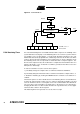
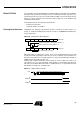
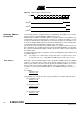
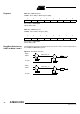
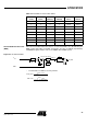
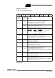
Table Of Contents
- Features
- Description
- Block Diagram
- SFR Mapping
- Pin Configurations
- Oscillators
- Enhanced Features
- Dual Data Pointer Register DPTR
- Expanded RAM (XRAM)
- Reset
- Power Monitor
- Timer 2
- Programmable Counter Array PCA
- Serial I/O Port
- Interrupt System
- Power Management
- Keyboard Interface
- 2-wire Interface (TWI)
- Serial Port Interface (SPI)
- Hardware Watchdog Timer
- ONCE(TM) Mode (ON Chip Emulation)
- Power-off Flag
- EEPROM Data Memory
- Reduced EMI Mode
- Flash Memory
- Electrical Characteristics
- Absolute Maximum Ratings
- DC Parameters
- AC Parameters
- Explanation of the AC Symbols
- External Program Memory Characteristics
- External Program Memory Read Cycle
- External Data Memory Characteristics
- External Data Memory Write Cycle
- External Data Memory Read Cycle
- Serial Port Timing - Shift Register Mode
- Shift Register Timing Waveforms
- External Clock Drive Waveforms
- AC Testing Input/Output Waveforms
- Float Waveforms
- Clock Waveforms
- Ordering Information
- Packaging Information
- Table of Contents
55
AT89C51ID2
4289C–8051–11/05
Registers Table 35. SADEN Register
SADEN - Slave Address Mask Register (B9h)
Reset Value = 0000 0000b
Not bit addressable
Table 36. SADDR Register
SADDR - Slave Address Register (A9h)
Reset Value = 0000 0000b
Not bit addressable
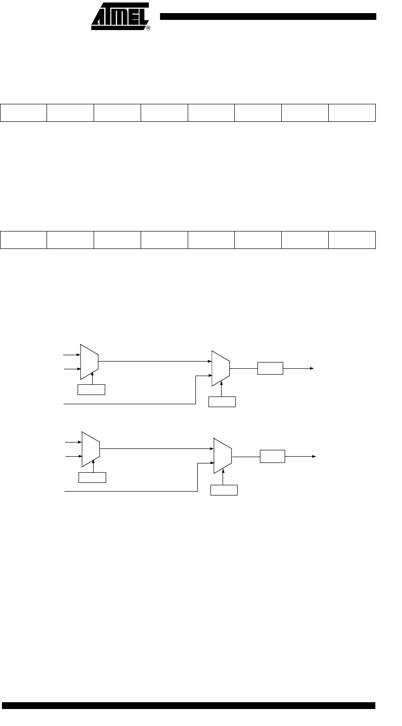
Baud Rate Selection for
UART for Mode 1 and 3
The Baud Rate Generator for transmit and receive clocks can be selected separately via
the T2CON and BDRCON registers.
Figure 23. Baud Rate Selection
76543210
76543210
RCLK
/ 16
RBCK
INT_BRG
0
1
TIMER1
0
1
0
1
TIMER2
INT_BRG
TIMER1
TIMER2
TIMER_BRG_RX
Rx Clock
/ 16
0
1
TIMER_BRG_TX
Tx Clock
TBCK
TCLK