
Datasheet
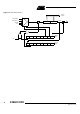
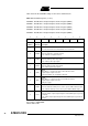
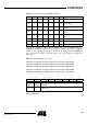
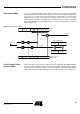
Table Of Contents
- Features
- Description
- Block Diagram
- SFR Mapping
- Pin Configurations
- Oscillators
- Enhanced Features
- Dual Data Pointer Register DPTR
- Expanded RAM (XRAM)
- Reset
- Power Monitor
- Timer 2
- Programmable Counter Array PCA
- Serial I/O Port
- Interrupt System
- Power Management
- Keyboard Interface
- 2-wire Interface (TWI)
- Serial Port Interface (SPI)
- Hardware Watchdog Timer
- ONCE(TM) Mode (ON Chip Emulation)
- Power-off Flag
- EEPROM Data Memory
- Reduced EMI Mode
- Flash Memory
- Electrical Characteristics
- Absolute Maximum Ratings
- DC Parameters
- AC Parameters
- Explanation of the AC Symbols
- External Program Memory Characteristics
- External Program Memory Read Cycle
- External Data Memory Characteristics
- External Data Memory Write Cycle
- External Data Memory Read Cycle
- Serial Port Timing - Shift Register Mode
- Shift Register Timing Waveforms
- External Clock Drive Waveforms
- AC Testing Input/Output Waveforms
- Float Waveforms
- Clock Waveforms
- Ordering Information
- Packaging Information
- Table of Contents
44
AT89C51ID2
4289C–8051–11/05
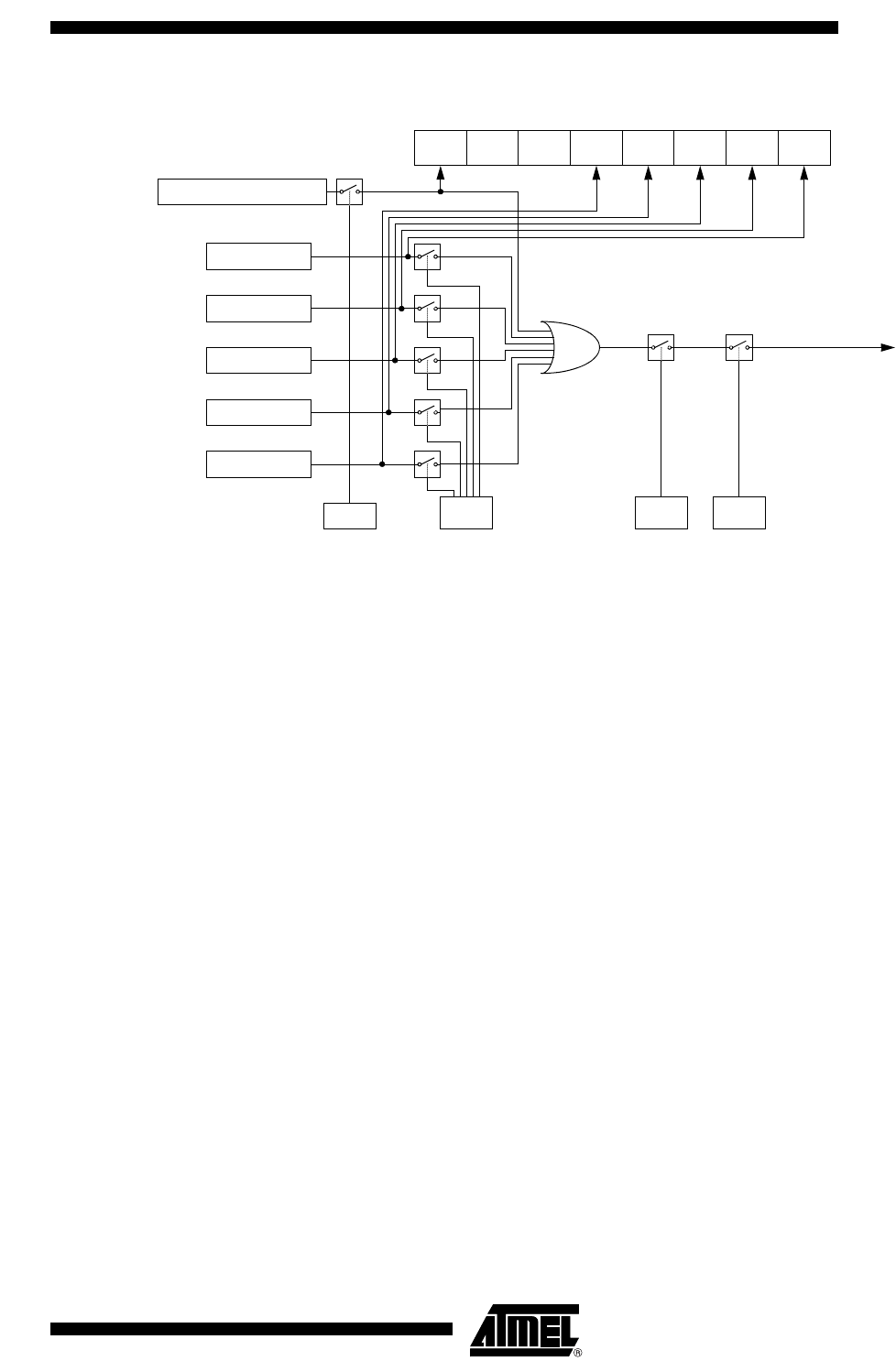
Figure 15. PCA Interrupt System
PCA Modules: each one of the five compare/capture modules has six possible func-
tions. It can perform:
• 16-bit Capture, positive-edge triggered
• 16-bit Capture, negative-edge triggered
• 16-bit Capture, both positive and negative-edge triggered
• 16-bit Software Timer
• 16-bit High Speed Output
• 8-bit Pulse Width Modulator
In addition, module 4 can be used as a Watchdog Timer.
Each module in the PCA has a special function register associated with it. These regis-
ters are: CCAPM0 for module 0, CCAPM1 for module 1, etc. (See Table 29). The
registers contain the bits that control the mode that each module will operate in.
• The ECCF bit (CCAPMn.0 where n=0, 1, 2, 3, or 4 depending on the module)
enables the CCF flag in the CCON SFR to generate an interrupt when a match or
compare occurs in the associated module.
• PWM (CCAPMn.1) enables the pulse width modulation mode.
• The TOG bit (CCAPMn.2) when set causes the CEX output associated with the
module to toggle when there is a match between the PCA counter and the module's
capture/compare register.
• The match bit MAT (CCAPMn.3) when set will cause the CCFn bit in the CCON
register to be set when there is a match between the PCA counter and the module's
capture/compare register.
• The next two bits CAPN (CCAPMn.4) and CAPP (CCAPMn.5) determine the edge
that a capture input will be active on. The CAPN bit enables the negative edge, and
the CAPP bit enables the positive edge. If both bits are set both edges will be
enabled and a capture will occur for either transition.
• The last bit in the register ECOM (CCAPMn.6) when set enables the comparator
function.
CF CR
CCON
0xD8
CCF4 CCF3 CCF2 CCF1 CCF0
Module 4
Module 3
Module 2
Module 1
Module 0
ECF
PCA Timer/Counter
ECCFn
CCAPMn.0CMOD.0
IEN0.6 IEN0.7
To Interrupt
priority decoder
EC EA