
Datasheet
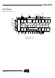
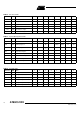
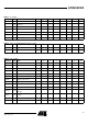

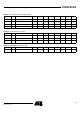

Table Of Contents
- Features
- Description
- Block Diagram
- SFR Mapping
- Pin Configurations
- Oscillators
- Enhanced Features
- Dual Data Pointer Register DPTR
- Expanded RAM (XRAM)
- Reset
- Power Monitor
- Timer 2
- Programmable Counter Array PCA
- Serial I/O Port
- Interrupt System
- Power Management
- Keyboard Interface
- 2-wire Interface (TWI)
- Serial Port Interface (SPI)
- Hardware Watchdog Timer
- ONCE(TM) Mode (ON Chip Emulation)
- Power-off Flag
- EEPROM Data Memory
- Reduced EMI Mode
- Flash Memory
- Electrical Characteristics
- Absolute Maximum Ratings
- DC Parameters
- AC Parameters
- Explanation of the AC Symbols
- External Program Memory Characteristics
- External Program Memory Read Cycle
- External Data Memory Characteristics
- External Data Memory Write Cycle
- External Data Memory Read Cycle
- Serial Port Timing - Shift Register Mode
- Shift Register Timing Waveforms
- External Clock Drive Waveforms
- AC Testing Input/Output Waveforms
- Float Waveforms
- Clock Waveforms
- Ordering Information
- Packaging Information
- Table of Contents

4
AT89C51ID2
4289C–8051–11/05
SFR Mapping The Special Function Registers (SFRs) of the AT89C51ID2 fall into the following
categories:
• C51 core registers: ACC, B, DPH, DPL, PSW, SP
• I/O port registers: P0, P1, P2, P3, PI2
• Timer registers: T2CON, T2MOD, TCON, TH0, TH1, TH2, TMOD, TL0, TL1, TL2,
RCAP2L, RCAP2H
• Serial I/O port registers: SADDR, SADEN, SBUF, SCON
• PCA (Programmable Counter Array) registers: CCON, CCAPMx, CL, CH, CCAPxH,
CCAPxL (x: 0 to 4)
• Power and clock control registers: PCON
• Hardware Watchdog Timer registers: WDTRST, WDTPRG
• Interrupt system registers: IE0, IPL0, IPH0, IE1, IPL1, IPH1
• Keyboard Interface registers: KBE, KBF, KBLS
• SPI registers: SPCON, SPSTR, SPDAT
• 2-wire Interface registers: SSCON, SSCS, SSDAT, SSADR
• BRG (Baud Rate Generator) registers: BRL, BDRCON
• Flash register: FCON
• Clock Prescaler register: CKRL
• 32 kHz Sub Clock Oscillator registers: CKSEL, OSSCON
• Others: AUXR, AUXR1, CKCON0, CKCON1