
Datasheet
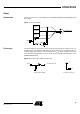

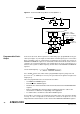
Table Of Contents
- Features
- Description
- Block Diagram
- SFR Mapping
- Pin Configurations
- Oscillators
- Enhanced Features
- Dual Data Pointer Register DPTR
- Expanded RAM (XRAM)
- Reset
- Power Monitor
- Timer 2
- Programmable Counter Array PCA
- Serial I/O Port
- Interrupt System
- Power Management
- Keyboard Interface
- 2-wire Interface (TWI)
- Serial Port Interface (SPI)
- Hardware Watchdog Timer
- ONCE(TM) Mode (ON Chip Emulation)
- Power-off Flag
- EEPROM Data Memory
- Reduced EMI Mode
- Flash Memory
- Electrical Characteristics
- Absolute Maximum Ratings
- DC Parameters
- AC Parameters
- Explanation of the AC Symbols
- External Program Memory Characteristics
- External Program Memory Read Cycle
- External Data Memory Characteristics
- External Data Memory Write Cycle
- External Data Memory Read Cycle
- Serial Port Timing - Shift Register Mode
- Shift Register Timing Waveforms
- External Clock Drive Waveforms
- AC Testing Input/Output Waveforms
- Float Waveforms
- Clock Waveforms
- Ordering Information
- Packaging Information
- Table of Contents
34
AT89C51ID2
4289C–8051–11/05
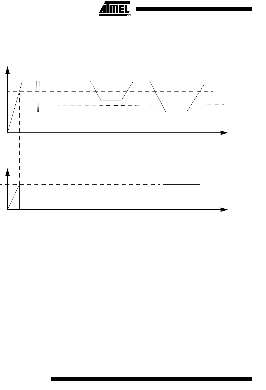
The Power fail detect monitor the supply generated by the voltage regulator and gener-
ate a reset if this supply falls below a safety threshold as illustrated in the Figure 11
below.
Figure 11. Power Fail Detect
When the power is applied, the Power Monitor immediately asserts a reset. Once the
internal supply after the voltage regulator reach a safety level, the power monitor then
looks at the XTAL clock input. The internal reset will remain asserted until the Xtal1 lev-
els are above and below VIH and VIL. Further more. An internal counter will count 1024
clock periods before the reset is de-asserted.
If the internal power supply falls below a safety level, a reset is immediately asserted.
Vcc
t
Reset
Vcc