
Datasheet
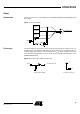
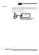

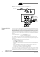
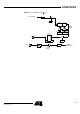
Table Of Contents
- Features
- Description
- Block Diagram
- SFR Mapping
- Pin Configurations
- Oscillators
- Enhanced Features
- Dual Data Pointer Register DPTR
- Expanded RAM (XRAM)
- Reset
- Power Monitor
- Timer 2
- Programmable Counter Array PCA
- Serial I/O Port
- Interrupt System
- Power Management
- Keyboard Interface
- 2-wire Interface (TWI)
- Serial Port Interface (SPI)
- Hardware Watchdog Timer
- ONCE(TM) Mode (ON Chip Emulation)
- Power-off Flag
- EEPROM Data Memory
- Reduced EMI Mode
- Flash Memory
- Electrical Characteristics
- Absolute Maximum Ratings
- DC Parameters
- AC Parameters
- Explanation of the AC Symbols
- External Program Memory Characteristics
- External Program Memory Read Cycle
- External Data Memory Characteristics
- External Data Memory Write Cycle
- External Data Memory Read Cycle
- Serial Port Timing - Shift Register Mode
- Shift Register Timing Waveforms
- External Clock Drive Waveforms
- AC Testing Input/Output Waveforms
- Float Waveforms
- Clock Waveforms
- Ordering Information
- Packaging Information
- Table of Contents
31
AT89C51ID2
4289C–8051–11/05
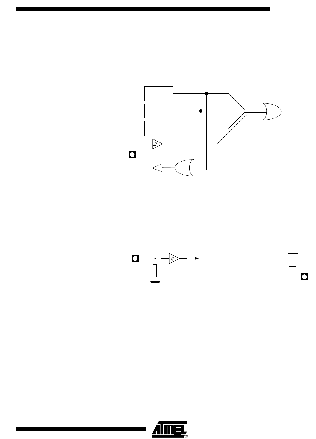
Reset
Introduction The reset sources are : Power Management, Hardware Watchdog, PCA Watchdog and
Reset input.
Figure 7. Reset schematic
Reset Input The Reset input can be used to force a reset pulse longer than the internal reset con-
trolled by the Power Monitor. RST input has a pull-down resistor allowing power-on
reset by simply connecting an external capacitor to V
CC
as shown in Figure 8. Resistor
value and input characteristics are discussed in the Section “DC Characteristics” of the
AT89C51ID2 datasheet.
Figure 8. Reset Circuitry and Power-On Reset
Power
Monitor
Hardware
Watchdog
PCA
Watchdog
RST
Internal Reset
RST
R
RST
VSS
To internal reset
RST
VDD
+
b. Power-on Reseta. RST input circuitry