
Datasheet
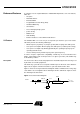

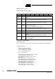

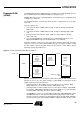
Table Of Contents
- Features
- Description
- Block Diagram
- SFR Mapping
- Pin Configurations
- Oscillators
- Enhanced Features
- Dual Data Pointer Register DPTR
- Expanded RAM (XRAM)
- Reset
- Power Monitor
- Timer 2
- Programmable Counter Array PCA
- Serial I/O Port
- Interrupt System
- Power Management
- Keyboard Interface
- 2-wire Interface (TWI)
- Serial Port Interface (SPI)
- Hardware Watchdog Timer
- ONCE(TM) Mode (ON Chip Emulation)
- Power-off Flag
- EEPROM Data Memory
- Reduced EMI Mode
- Flash Memory
- Electrical Characteristics
- Absolute Maximum Ratings
- DC Parameters
- AC Parameters
- Explanation of the AC Symbols
- External Program Memory Characteristics
- External Program Memory Read Cycle
- External Data Memory Characteristics
- External Data Memory Write Cycle
- External Data Memory Read Cycle
- Serial Port Timing - Shift Register Mode
- Shift Register Timing Waveforms
- External Clock Drive Waveforms
- AC Testing Input/Output Waveforms
- Float Waveforms
- Clock Waveforms
- Ordering Information
- Packaging Information
- Table of Contents
25
AT89C51ID2
4289C–8051–11/05
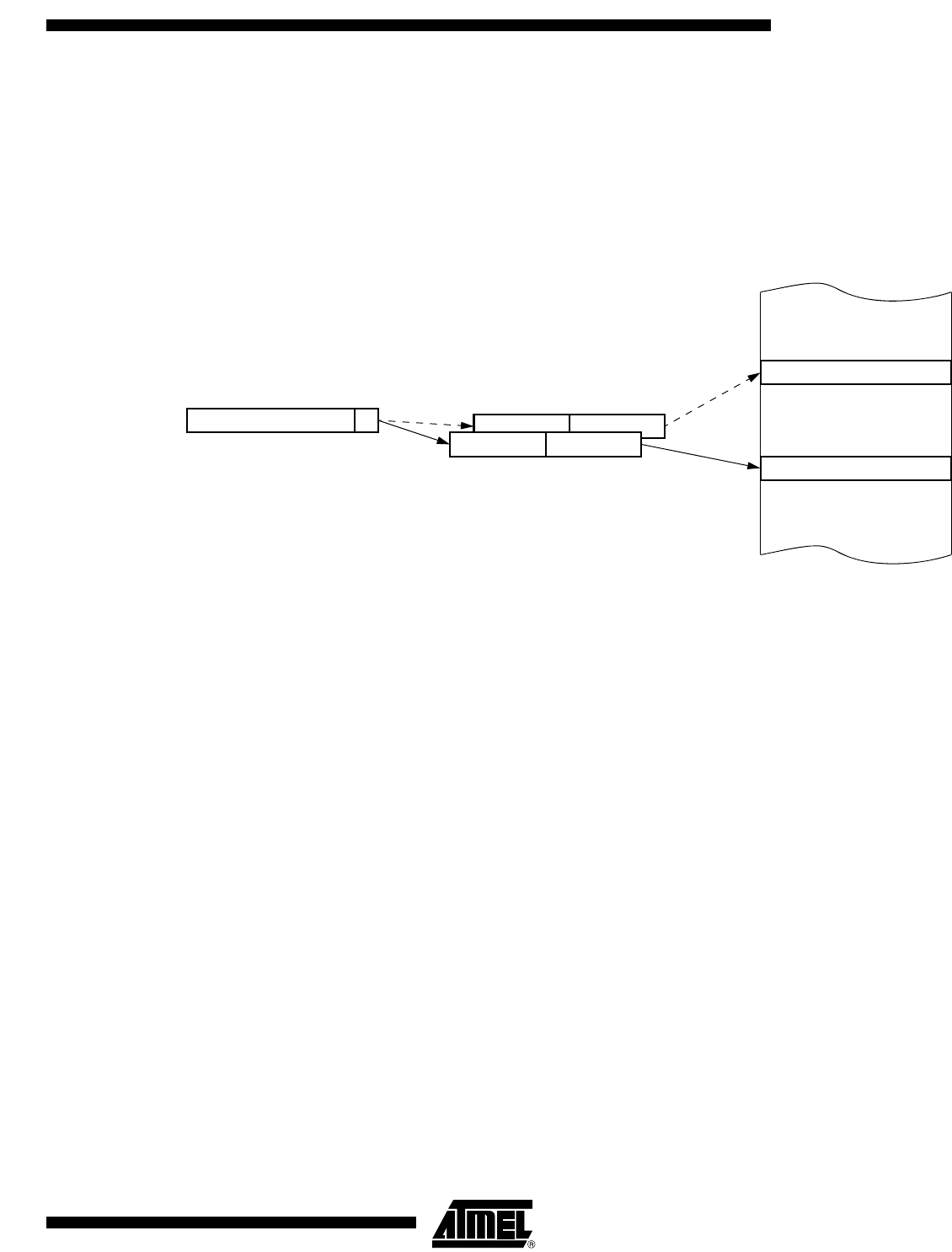
Dual Data Pointer
Register DPTR
The additional data pointer can be used to speed up code execution and reduce code
size.
The dual DPTR structure is a way by which the chip will specify the address of an exter-
nal data memory location. There are two 16-bit DPTR registers that address the external
memory, and a single bit called DPS = AUXR1.0 (see Table 23) that allows the program
code to switch between them (Refer to Figure 5).
Figure 5. Use of Dual Pointer
External Data Memory
AUXR1(A2H)
DPS
DPH(83H) DPL(82H)
07
DPTR0
DPTR1