
Datasheet

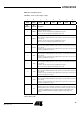
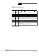
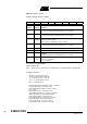
Table Of Contents
- Features
- Description
- Block Diagram
- SFR Mapping
- Pin Configurations
- Oscillators
- Enhanced Features
- Dual Data Pointer Register DPTR
- Expanded RAM (XRAM)
- Reset
- Power Monitor
- Timer 2
- Programmable Counter Array PCA
- Serial I/O Port
- Interrupt System
- Power Management
- Keyboard Interface
- 2-wire Interface (TWI)
- Serial Port Interface (SPI)
- Hardware Watchdog Timer
- ONCE(TM) Mode (ON Chip Emulation)
- Power-off Flag
- EEPROM Data Memory
- Reduced EMI Mode
- Flash Memory
- Electrical Characteristics
- Absolute Maximum Ratings
- DC Parameters
- AC Parameters
- Explanation of the AC Symbols
- External Program Memory Characteristics
- External Program Memory Read Cycle
- External Data Memory Characteristics
- External Data Memory Write Cycle
- External Data Memory Read Cycle
- Serial Port Timing - Shift Register Mode
- Shift Register Timing Waveforms
- External Clock Drive Waveforms
- AC Testing Input/Output Waveforms
- Float Waveforms
- Clock Waveforms
- Ordering Information
- Packaging Information
- Table of Contents

23
AT89C51ID2
4289C–8051–11/05
Table 21. CKCON0 Register
CKCON0 - Clock Control Register (8Fh)
Reset Value = 0000 000’HSB. X2’b (See “Hardware Security Byte”)
Not bit addressable
76543210
TWIX2 WDX2 PCAX2 SIX2 T2X2 T1X2 T0X2 X2
Bit
Number
Bit
Mnemonic Description
7TWIX2
2-wire clock (This control bit is validated when the CPU clock X2 is set; when X2
is low, this bit has no effect)
Cleared to select 6 clock periods per peripheral clock cycle.
Set to select 12 clock periods per peripheral clock cycle.
6WDX2
Watchdog Clock
(This control bit is validated when the CPU clock X2 is set; when X2 is low, this bit
has no effect).
Cleared to select 6 clock periods per peripheral clock cycle.
Set to select 12 clock periods per peripheral clock cycle.
5 PCAX2
Programmable Counter Array Clock
(This control bit is validated when the CPU clock X2 is set; when X2 is low, this bit
has no effect).
Cleared to select 6 clock periods per peripheral clock cycle. Set to select 12 clock
periods per peripheral clock cycle.
4SIX2
Enhanced UART Clock (Mode 0 and 2)
(This control bit is validated when the CPU clock X2 is set; when X2 is low, this bit
has no effect).
Cleared to select 6 clock periods per peripheral clock cycle. Set to select 12 clock
periods per peripheral clock cycle.
3T2X2
Timer2 Clock
(This control bit is validated when the CPU clock X2 is set; when X2 is low, this bit
has no effect).
Cleared to select 6 clock periods per peripheral clock cycle.
Set to select 12 clock periods per peripheral clock cycle.
2T1X2
Timer1 Clock
(This control bit is validated when the CPU clock X2 is set; when X2 is low, this bit
has no effect).
Cleared to select 6 clock periods per peripheral clock cycle. Set to select 12 clock
periods per peripheral clock cycle.
1T0X2
Timer0 Clock
(This control bit is validated when the CPU clock X2 is set; when X2 is low, this bit
has no effect).
Cleared to select 6 clock periods per peripheral clock cycle. Set to select 12 clock
periods per peripheral clock cycle.
0X2
CPU Clock
Cleared to select 12 clock periods per machine cycle (STD mode) for CPU and
all the peripherals. Set to select 6clock periods per machine cycle (X2 mode) and
to enable the individual peripherals’X2’ bits. Programmed by hardware after
Power-up regarding Hardware Security Byte (HSB), Default setting, X2 is
cleared.