
Datasheet
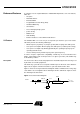

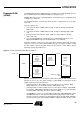
Table Of Contents
- Features
- Description
- Block Diagram
- SFR Mapping
- Pin Configurations
- Oscillators
- Enhanced Features
- Dual Data Pointer Register DPTR
- Expanded RAM (XRAM)
- Reset
- Power Monitor
- Timer 2
- Programmable Counter Array PCA
- Serial I/O Port
- Interrupt System
- Power Management
- Keyboard Interface
- 2-wire Interface (TWI)
- Serial Port Interface (SPI)
- Hardware Watchdog Timer
- ONCE(TM) Mode (ON Chip Emulation)
- Power-off Flag
- EEPROM Data Memory
- Reduced EMI Mode
- Flash Memory
- Electrical Characteristics
- Absolute Maximum Ratings
- DC Parameters
- AC Parameters
- Explanation of the AC Symbols
- External Program Memory Characteristics
- External Program Memory Read Cycle
- External Data Memory Characteristics
- External Data Memory Write Cycle
- External Data Memory Read Cycle
- Serial Port Timing - Shift Register Mode
- Shift Register Timing Waveforms
- External Clock Drive Waveforms
- AC Testing Input/Output Waveforms
- Float Waveforms
- Clock Waveforms
- Ordering Information
- Packaging Information
- Table of Contents
22
AT89C51ID2
4289C–8051–11/05
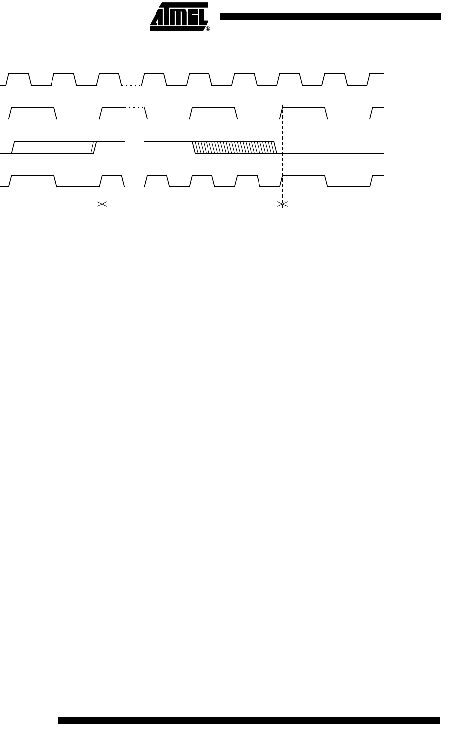
Figure 4. Mode Switching Waveforms
The X2 bit in the CKCON0 register (see Table 21) allows a switch from 12 clock periods
per instruction to 6 clock periods and vice versa. At reset, the speed is set according to
X2 bit of Hardware Security Byte (HSB). By default, Standard mode is active. Setting the
X2 bit activates the X2 feature (X2 mode).
The T0X2, T1X2, T2X2, UartX2, PcaX2, and WdX2 bits in the CKCON0 register (See
Table 21.) and SPIX2 bit in the CKCON1 register (see Table 22) allows a switch from
standard peripheral speed (12 clock periods per peripheral clock cycle) to fast periph-
eral speed (6 clock periods per peripheral clock cycle). These bits are active only in X2
mode.
XTAL1:2
XTAL1
CPU clock
X2 bit
X2 ModeSTD Mode STD Mode
F
OSC