
Datasheet
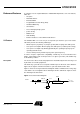

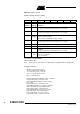
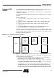
Table Of Contents
- Features
- Description
- Block Diagram
- SFR Mapping
- Pin Configurations
- Oscillators
- Enhanced Features
- Dual Data Pointer Register DPTR
- Expanded RAM (XRAM)
- Reset
- Power Monitor
- Timer 2
- Programmable Counter Array PCA
- Serial I/O Port
- Interrupt System
- Power Management
- Keyboard Interface
- 2-wire Interface (TWI)
- Serial Port Interface (SPI)
- Hardware Watchdog Timer
- ONCE(TM) Mode (ON Chip Emulation)
- Power-off Flag
- EEPROM Data Memory
- Reduced EMI Mode
- Flash Memory
- Electrical Characteristics
- Absolute Maximum Ratings
- DC Parameters
- AC Parameters
- Explanation of the AC Symbols
- External Program Memory Characteristics
- External Program Memory Read Cycle
- External Data Memory Characteristics
- External Data Memory Write Cycle
- External Data Memory Read Cycle
- Serial Port Timing - Shift Register Mode
- Shift Register Timing Waveforms
- External Clock Drive Waveforms
- AC Testing Input/Output Waveforms
- Float Waveforms
- Clock Waveforms
- Ordering Information
- Packaging Information
- Table of Contents
21
AT89C51ID2
4289C–8051–11/05
Enhanced Features In comparison to the original 80C52, the AT89C51ID2 implements some new features,
which are
:
• X2 option
• Dual Data Pointer
• Extended RAM
• Programmable Counter Array (PCA)
• Hardware Watchdog
• SPI interface
• 4-level interrupt priority system
• power-off flag
• ONCE mode
• ALE disabling
• Enhanced features on the UART and the timer 2
X2 Feature The AT89C51ID2 core needs only 6 clock periods per machine cycle. This feature
called ‘X2’ provides the following advantages:
• Divide frequency crystals by 2 (cheaper crystals) while keeping same CPU power.
• Save power consumption while keeping same CPU power (oscillator power saving).
• Save power consumption by dividing dynamically the operating frequency by 2 in
operating and idle modes.
• Increase CPU power by 2 while keeping same crystal frequency.
In order to keep the original C51 compatibility, a divider by 2 is inserted between the
XTAL1 signal and the main clock input of the core (phase generator). This divider may
be disabled by software.
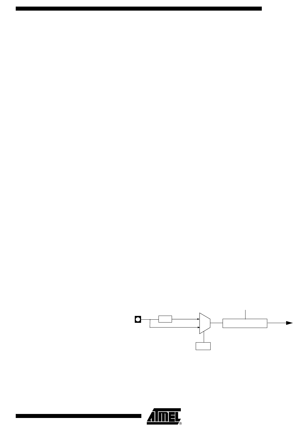
Description The clock for the whole circuit and peripherals is first divided by two before being used
by the CPU core and the peripherals.
This allows any cyclic ratio to be accepted on XTAL1 input. In X2 mode, as this divider is
bypassed, the signals on XTAL1 must have a cyclic ratio between 40 to 60%.
Figure 3 shows the clock generation block diagram. X2 bit is validated on the rising edge
of the XTAL1÷2 to avoid glitches when switching from X2 to STD mode. Figure 4 shows
the switching mode waveforms.
Figure 3. Clock Generation Diagram
XTAL1
2
CKCON0
X2
8 bit Prescaler
F
OSC
FXTAL
0
1
XTAL1:2
F
CLK CPU
F
CLK PERIPH
CKRL