
Datasheet
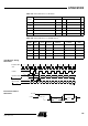
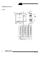
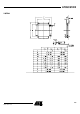

Table Of Contents
- Features
- Description
- Block Diagram
- SFR Mapping
- Pin Configurations
- Oscillators
- Enhanced Features
- Dual Data Pointer Register DPTR
- Expanded RAM (XRAM)
- Reset
- Power Monitor
- Timer 2
- Programmable Counter Array PCA
- Serial I/O Port
- Interrupt System
- Power Management
- Keyboard Interface
- 2-wire Interface (TWI)
- Serial Port Interface (SPI)
- Hardware Watchdog Timer
- ONCE(TM) Mode (ON Chip Emulation)
- Power-off Flag
- EEPROM Data Memory
- Reduced EMI Mode
- Flash Memory
- Electrical Characteristics
- Absolute Maximum Ratings
- DC Parameters
- AC Parameters
- Explanation of the AC Symbols
- External Program Memory Characteristics
- External Program Memory Read Cycle
- External Data Memory Characteristics
- External Data Memory Write Cycle
- External Data Memory Read Cycle
- Serial Port Timing - Shift Register Mode
- Shift Register Timing Waveforms
- External Clock Drive Waveforms
- AC Testing Input/Output Waveforms
- Float Waveforms
- Clock Waveforms
- Ordering Information
- Packaging Information
- Table of Contents

i
AT89C51ID2
4289C–8051–11/05
Table of Contents
Features................................................................................................. 1
Description............................................................................................ 1
Block Diagram....................................................................................... 3
SFR Mapping......................................................................................... 4
Pin Configurations.............................................................................. 10
Oscillators ........................................................................................... 14
Overview............................................................................................................. 14
Registers............................................................................................................. 14
Functional Block Diagram................................................................................... 17
Operating Modes ................................................................................................ 17
Design Considerations........................................................................................ 19
Timer 0: Clock Inputs.......................................................................................... 20
Enhanced Features............................................................................. 21
X2 Feature.......................................................................................................... 21
Dual Data Pointer Register DPTR...................................................... 25
Expanded RAM (XRAM) ..................................................................... 28
Registers............................................................................................................. 30
Reset.................................................................................................... 31
Introduction......................................................................................................... 31
Reset Input ......................................................................................................... 31
Reset Output....................................................................................................... 32
Power Monitor..................................................................................... 33
Description.......................................................................................................... 33
Timer 2................................................................................................. 35
Auto-Reload Mode.............................................................................................. 35
Programmable Clock-Output .............................................................................. 36
Registers............................................................................................................. 38
Programmable Counter Array PCA................................................... 40
PCA Capture Mode............................................................................................. 48
16-bit Software Timer/ Compare Mode............................................................... 48
High Speed Output Mode ................................................................................... 49
Pulse Width Modulator Mode.............................................................................. 50