
Datasheet
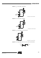

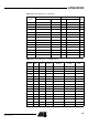
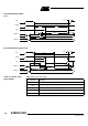
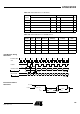
Table Of Contents
- Features
- Description
- Block Diagram
- SFR Mapping
- Pin Configurations
- Oscillators
- Enhanced Features
- Dual Data Pointer Register DPTR
- Expanded RAM (XRAM)
- Reset
- Power Monitor
- Timer 2
- Programmable Counter Array PCA
- Serial I/O Port
- Interrupt System
- Power Management
- Keyboard Interface
- 2-wire Interface (TWI)
- Serial Port Interface (SPI)
- Hardware Watchdog Timer
- ONCE(TM) Mode (ON Chip Emulation)
- Power-off Flag
- EEPROM Data Memory
- Reduced EMI Mode
- Flash Memory
- Electrical Characteristics
- Absolute Maximum Ratings
- DC Parameters
- AC Parameters
- Explanation of the AC Symbols
- External Program Memory Characteristics
- External Program Memory Read Cycle
- External Data Memory Characteristics
- External Data Memory Write Cycle
- External Data Memory Read Cycle
- Serial Port Timing - Shift Register Mode
- Shift Register Timing Waveforms
- External Clock Drive Waveforms
- AC Testing Input/Output Waveforms
- Float Waveforms
- Clock Waveforms
- Ordering Information
- Packaging Information
- Table of Contents
150
AT89C51ID2
4289C–8051–11/05
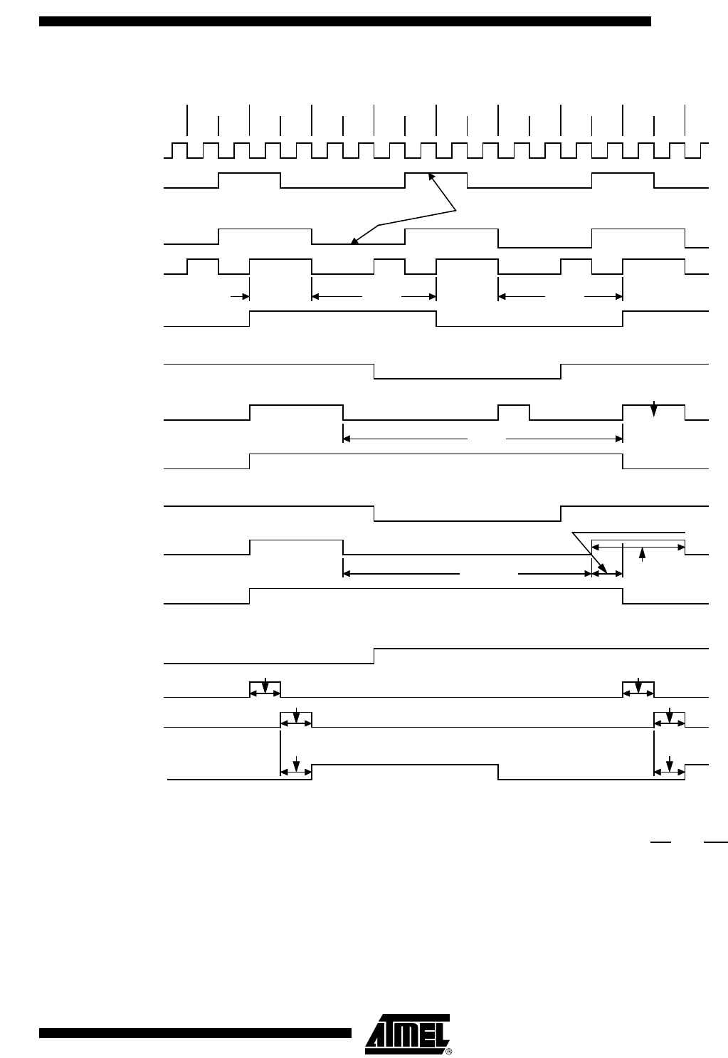
Figure 61. Internal Clock Signals
This diagram indicates when signals are clocked internally. The time it takes the signals to propagate to the pins, however,
ranges from 25 to 125 ns. This propagation delay is dependent on variables such as temperature and pin loading. Propaga-
tion also varies from output to output and component. Typically though (T
A
= 25°C fully loaded) RD and WR propagation
delays are approximately 50 ns. The other signals are typically 85 ns. Propagation delays are incorporated in the AC
specifications.
DATA PCL OUT DATA PCL OUT DATA PCL OUT
SAMPLED SAMPLED SAMPLED
STATE4 STATE5 STATE6 STATE1 STATE2 STATE3 STATE4 STATE5
P1 P2 P1 P2 P1 P2 P1 P2 P1 P2 P1 P2 P1 P2 P1 P2
FLOAT FLOAT FLOAT
THESE SIGNALS ARE NOT ACTIVATED DURING THE
EXECUTION OF A MOVX INSTRUCTION
INDICATES ADDRESS TRANSITIONS
EXTERNAL PROGRAM MEMORY FETCH
FLOAT
DATA
SAMPLED
DPL OR Rt OUT
INDICATES DPH OR P2 SFR TO PCH TRANSITION
PCL OUT (IF PROGRAM
MEMORY IS EXTERNAL)
PCL OUT (EVEN IF PROGRAM
MEMORY IS INTERNAL)
PCL OUT (IF PROGRAM
MEMORY IS EXTERNAL
)
OLD DATA
NEW DATA
P0 PINS SAMPLED
P1, P2, P3 PINS SAMPLED P1, P2, P3 PINS SAMPLED
P0 PINS SAMPLED
RXD SAMPLED
INTERNAL
CLOCK
XTAL2
ALE
PSEN
P0
P2 (EXT)
READ CYCLE
WRITE CYCLE
RD
P0
P2
WR
PORT OPERATION
MOV PORT SRC
MOV DEST P0
MOV DEST PORT (P1. P2. P3)
(INCLUDES INTO. INT1. TO T1)
SERIAL PORT SHIFT CLOCK
TXD (MODE 0)
DATA OUT
DPL OR Rt OUT
INDICATES DPH OR P2 SFR TO PCH TRANSITION
P0
P2
RXD SAMPLED