
Datasheet
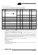
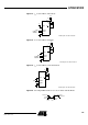

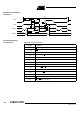
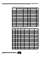
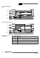
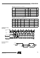
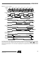
Table Of Contents
- Features
- Description
- Block Diagram
- SFR Mapping
- Pin Configurations
- Oscillators
- Enhanced Features
- Dual Data Pointer Register DPTR
- Expanded RAM (XRAM)
- Reset
- Power Monitor
- Timer 2
- Programmable Counter Array PCA
- Serial I/O Port
- Interrupt System
- Power Management
- Keyboard Interface
- 2-wire Interface (TWI)
- Serial Port Interface (SPI)
- Hardware Watchdog Timer
- ONCE(TM) Mode (ON Chip Emulation)
- Power-off Flag
- EEPROM Data Memory
- Reduced EMI Mode
- Flash Memory
- Electrical Characteristics
- Absolute Maximum Ratings
- DC Parameters
- AC Parameters
- Explanation of the AC Symbols
- External Program Memory Characteristics
- External Program Memory Read Cycle
- External Data Memory Characteristics
- External Data Memory Write Cycle
- External Data Memory Read Cycle
- Serial Port Timing - Shift Register Mode
- Shift Register Timing Waveforms
- External Clock Drive Waveforms
- AC Testing Input/Output Waveforms
- Float Waveforms
- Clock Waveforms
- Ordering Information
- Packaging Information
- Table of Contents
143
AT89C51ID2
4289C–8051–11/05
AC Parameters
Explanation of the AC
Symbols
Each timing symbol has 5 characters. The first character is always a “T” (stands for
time). The other characters, depending on their positions, stand for the name of a signal
or the logical status of that signal. The following is a list of all the characters and what
they stand for.
Example:T
AVLL
= Time for Address Valid to ALE Low.
T
LLPL
= Time for ALE Low to PSEN Low.
(Load Capacitance for port 0, ALE and PSEN = 100 pF; Load Capacitance for all other
outputs = 80 pF.)
Table 98 Table 101, and Table 104 give the description of each AC symbols.
Table 99, Table 100, Table 102 and Table 105 gives the range for each AC parameter.
Table 99, Table 100 and Table 106 give the frequency derating formula of the AC
parameter for each speed range description. To calculate each AC symbols. take the x
value in the correponding column (-M or -L) and use this value in the formula.
Example: T
LLIU
for -M and 20 MHz, Standard clock.
x = 35 ns
T 50 ns
T
CCIV
= 4T - x = 165 ns
External Program Memory
Characteristics
Table 98. Symbol Description
Symbol Parameter
T Oscillator clock period
T
LHLL
ALE pulse width
T
AVLL
Address Valid to ALE
T
LLAX
Address Hold After ALE
T
LLIV
ALE to Valid Instruction In
T
LLPL
ALE to PSEN
T
PLPH
PSEN Pulse Width
T
PLIV
PSEN to Valid Instruction In
T
PXIX
Input Instruction Hold After PSEN
T
PXIZ
Input Instruction Float After PSEN
T
AVIV
Address to Valid Instruction In
T
PLAZ
PSEN Low to Address Float