
Datasheet
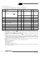

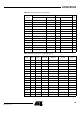
Table Of Contents
- Features
- Description
- Block Diagram
- SFR Mapping
- Pin Configurations
- Oscillators
- Enhanced Features
- Dual Data Pointer Register DPTR
- Expanded RAM (XRAM)
- Reset
- Power Monitor
- Timer 2
- Programmable Counter Array PCA
- Serial I/O Port
- Interrupt System
- Power Management
- Keyboard Interface
- 2-wire Interface (TWI)
- Serial Port Interface (SPI)
- Hardware Watchdog Timer
- ONCE(TM) Mode (ON Chip Emulation)
- Power-off Flag
- EEPROM Data Memory
- Reduced EMI Mode
- Flash Memory
- Electrical Characteristics
- Absolute Maximum Ratings
- DC Parameters
- AC Parameters
- Explanation of the AC Symbols
- External Program Memory Characteristics
- External Program Memory Read Cycle
- External Data Memory Characteristics
- External Data Memory Write Cycle
- External Data Memory Read Cycle
- Serial Port Timing - Shift Register Mode
- Shift Register Timing Waveforms
- External Clock Drive Waveforms
- AC Testing Input/Output Waveforms
- Float Waveforms
- Clock Waveforms
- Ordering Information
- Packaging Information
- Table of Contents
141
AT89C51ID2
4289C–8051–11/05
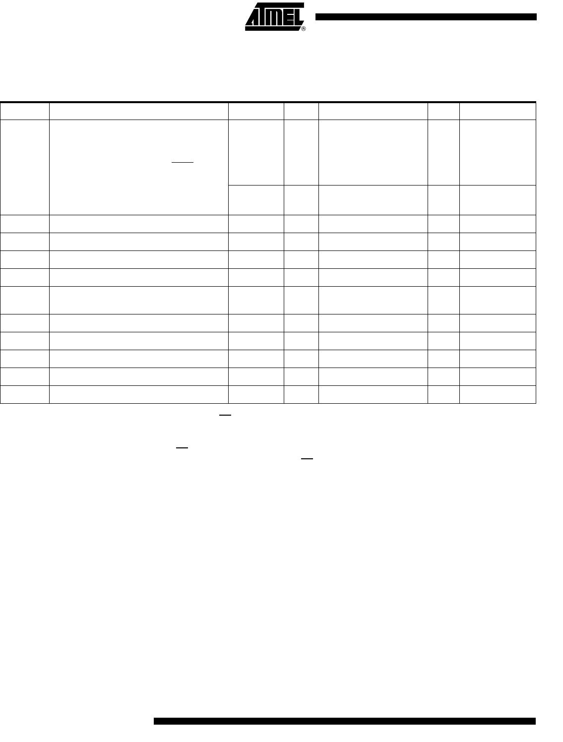
Notes: 1. Operating I
CC
is measured with all output pins disconnected; XTAL1 driven with T
CLCH
, T
CHCL
= 5 ns (see Figure 60), V
IL
=
V
SS
+ 0.5V, V
IH
= V
CC
- 0.5V; XTAL2 N.C.; EA = RST = Port 0 = V
CC
. I
CC
would be slightly higher if a crystal oscillator used
(see Figure 57).
2. Idle I
CC
is measured with all output pins disconnected; XTAL1 driven with T
CLCH
, T
CHCL
= 5 ns, V
IL
= V
SS
+ 0.5V, V
IH
= V
CC
-
0.5V; XTAL2 N.C; Port 0 = V
CC
; EA = RST = V
SS
(see Figure 58).
3. Power-down I
CC
is measured with all output pins disconnected; EA = V
CC
, PORT 0 = V
CC
; XTAL2 NC.; RST = V
SS
(see Fig-
ure 59).
4. Capacitance loading on Ports 0 and 2 may cause spurious noise pulses to be superimposed on the V
OLS
of ALE and Ports 1
and 3. The noise is due to external bus capacitance discharging into the Port 0 and Port 2 pins when these pins make 1 to 0
transitions during bus operation. In the worst cases (capacitive loading 100 pF), the noise pulse on the ALE line may exceed
0.45V with maxi V
OL
peak 0.6V. A Schmitt Trigger use is not necessary.
5. Typical values are based on a limited number of samples and are not guaranteed. The values listed are at room temperature
and 5V.
6. Under steady state (non-transient) conditions, I
OL
must be externally limited as follows:
Maximum I
OL
per port pin: 10 mA
Maximum I
OL
per 8-bit port:
Port 0: 26 mA
Ports 1, 2 and 3: 15 mA
Maximum total I
OL
for all output pins: 71 mA
If I
OL
exceeds the test condition, V
OL
may exceed the related specification. Pins are not guaranteed to sink current greater
than the listed test conditions.
V
OH1
Output High Voltage, port 0, ALE, PSEN
V
CC
- 0.3
V
CC
- 0.7
V
CC
- 1.5
V
V
V
V
CC
= 5V ± 10%
I
OH
= -200 μA
I
OH
= -3.2 mA
I
OH
= -7.0 mA
0.9 V
CC
V
V
CC
= 2.7V to 5.5V
I
OH
= -10 μA
R
RST
RST Pull-down Resistor 50 200
(5)
250 kΩ
I
IL
Logical 0 Input Current ports 1, 2, 3, 4 and 5 -50 μAV
IN
= 0.45V
I
LI
Input Leakage Current ±10 μA 0.45V < V
IN
< V
CC
I
TL
Logical 1 to 0 Transition Current, ports 1, 2, 3, 4 -650 μAV
IN
= 2.0V
C
IO
Capacitance of I/O Buffer 10 pF
F
C
= 3 MHz
T
A
= 25°C
I
PD
Power-down Current 75 150 μA 2.7 < V
CC <
5.5V
(3)
I
CCOP
Power Supply Current on normal mode 0.4 x Frequency (MHz) + 5 mA V
CC
= 5.5V
(1)
I
CCIDLE
Power Supply Current on idle mode 0.3 x Frequency (MHz) + 5 mA V
CC
= 5.5V
(2)
I
CCWRITE
Power Supply Current on flash or EEdata write 0.8 x Frequency (MHz) + 15 mA V
CC
= 5.5V
t
WRITE
Flash or EEdata programming time 7 10 ms 2.7 < V
CC <
5.5V
T
A
= -40°C to +85°C; V
SS
= 0V;
V
CC
=2.7V to 5.5V and F = 0 to 40 MHz (both internal and external code execution)
V
CC
=4.5V to 5.5V and F = 0 to 60 MHz (internal code execution only) (Continued)
Symbol Parameter Min Typ Max Unit Test Conditions