
Datasheet
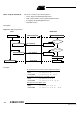
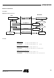
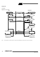
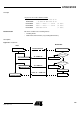
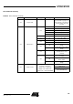
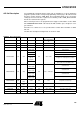

Table Of Contents
- Features
- Description
- Block Diagram
- SFR Mapping
- Pin Configurations
- Oscillators
- Enhanced Features
- Dual Data Pointer Register DPTR
- Expanded RAM (XRAM)
- Reset
- Power Monitor
- Timer 2
- Programmable Counter Array PCA
- Serial I/O Port
- Interrupt System
- Power Management
- Keyboard Interface
- 2-wire Interface (TWI)
- Serial Port Interface (SPI)
- Hardware Watchdog Timer
- ONCE(TM) Mode (ON Chip Emulation)
- Power-off Flag
- EEPROM Data Memory
- Reduced EMI Mode
- Flash Memory
- Electrical Characteristics
- Absolute Maximum Ratings
- DC Parameters
- AC Parameters
- Explanation of the AC Symbols
- External Program Memory Characteristics
- External Program Memory Read Cycle
- External Data Memory Characteristics
- External Data Memory Write Cycle
- External Data Memory Read Cycle
- Serial Port Timing - Shift Register Mode
- Shift Register Timing Waveforms
- External Clock Drive Waveforms
- AC Testing Input/Output Waveforms
- Float Waveforms
- Clock Waveforms
- Ordering Information
- Packaging Information
- Table of Contents
140
AT89C51ID2
4289C–8051–11/05
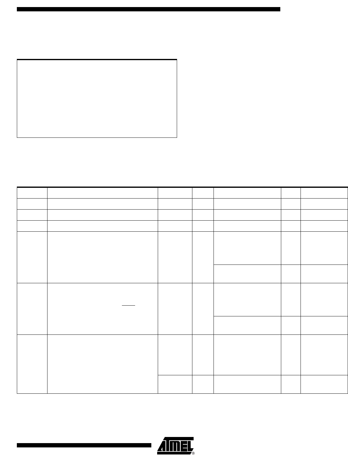
Electrical Characteristics
Absolute Maximum Ratings
DC Parameters
I = industrial ........................................................-40°C to 85°C
Storage Temperature .................................... -65°C to + 150°C
Voltage on V
CC
to V
SS
(standard voltage) .........-0.5V to + 6.5V
Voltage on V
CC
to V
SS
(low voltage)..................-0.5V to + 4.5V
Voltage on Any Pin to V
SS
..........................-0.5V to V
CC
+ 0.5V
Power Dissipation........................................................... 1 W
(2)
Note: Stresses at or above those listed under “Absolute
Maximum Ratings” may cause permanent damage to
the device. This is a stress rating only and functional
operation of the device at these or any other condi-
tions above those indicated in the operational
sections of this specification is not implied. Exposure
to absolute maximum rating conditions may affect
device reliability.
Power dissipation is based on the maximum allow-
able die temperature and the thermal resistance of
the package.
T
A
= -40°C to +85°C; V
SS
= 0V;
V
CC
=2.7V to 5.5V and F = 0 to 40 MHz (both internal and external code execution)
V
CC
=4.5V to 5.5V and F = 0 to 60 MHz (internal code execution only)
Symbol Parameter Min Typ Max Unit Test Conditions
V
IL
Input Low Voltage -0.5 0.2 V
CC
- 0.1 V
V
IH
Input High Voltage except RST, XTAL1 0.2 V
CC
+ 0.9 V
CC
+ 0.5 V
V
IH1
Input High Voltage RST, XTAL1 0.7 V
CC
V
CC
+ 0.5 V
V
OL
Output Low Voltage, ports 1, 2, 3, 4
(6)
0.3
0.45
1.0
V
V
V
V
CC
= 4.5V to 5.5V
I
OL
= 100 μA
(4)
I
OL
= 1.6 mA
(4)
I
OL
= 3.5 mA
(4)
0.45 V
V
CC
= 2.7V to 5.5V
I
OL
= 0.8 mA
(4)
V
OL1
Output Low Voltage, port 0, ALE, PSEN
(6)
0.3
0.45
1.0
V
V
V
V
CC
= 4.5V to 5.5V
I
OL
= 200 μA
(4)
I
OL
= 3.2 mA
(4)
I
OL
= 7.0 mA
(4)
0.45 V
V
CC
= 2.7V to 5.5V
I
OL
= 1.6 mA
(4)
V
OH
Output High Voltage, ports 1, 2, 3, 4
V
CC
- 0.3
V
CC
- 0.7
V
CC
- 1.5
V
V
V
V
CC
= 5V ± 10%
I
OH
= -10 μA
I
OH
= -30 μA
I
OH
= -60 μA
0.9 V
CC
V
V
CC
= 2.7V to 5.5V
I
OH
= -10 μA