
Datasheet
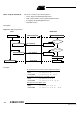
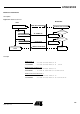
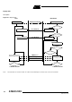
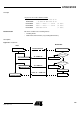

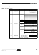
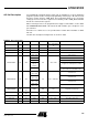

Table Of Contents
- Features
- Description
- Block Diagram
- SFR Mapping
- Pin Configurations
- Oscillators
- Enhanced Features
- Dual Data Pointer Register DPTR
- Expanded RAM (XRAM)
- Reset
- Power Monitor
- Timer 2
- Programmable Counter Array PCA
- Serial I/O Port
- Interrupt System
- Power Management
- Keyboard Interface
- 2-wire Interface (TWI)
- Serial Port Interface (SPI)
- Hardware Watchdog Timer
- ONCE(TM) Mode (ON Chip Emulation)
- Power-off Flag
- EEPROM Data Memory
- Reduced EMI Mode
- Flash Memory
- Electrical Characteristics
- Absolute Maximum Ratings
- DC Parameters
- AC Parameters
- Explanation of the AC Symbols
- External Program Memory Characteristics
- External Program Memory Read Cycle
- External Data Memory Characteristics
- External Data Memory Write Cycle
- External Data Memory Read Cycle
- Serial Port Timing - Shift Register Mode
- Shift Register Timing Waveforms
- External Clock Drive Waveforms
- AC Testing Input/Output Waveforms
- Float Waveforms
- Clock Waveforms
- Ordering Information
- Packaging Information
- Table of Contents

139
AT89C51ID2
4289C–8051–11/05
PROGRAM DATA
PAGE
09h
Number of
byte to
program
Address of
the first byte
to program in
the Flash
memory
Address in
XRAM of the
first data to
program
ACC = 0: DONE
Program up to 128 bytes in user Flash.
Remark: number of bytes to program is
limited such as the Flash write remains in a
single 128 bytes page. Hence, when ACC
is 128, valid values of DPL are 00h, or, 80h.
PROGRAM X2 FUSE 0Ah
Fuse value
00h or 01h
0008h XXh none Program X2 fuse bit with ACC
PROGRAM BLJB
FUSE
0Ah
Fuse value
00h or 01h
0004h XXh none Program BLJB fuse bit with ACC
READ HSB 0Bh XXh XXXXh XXh ACC = HSB Read Hardware Byte
READ BOOT ID1 0Eh XXh DPL = 00h XXh ACC = ID1 Read boot ID1
READ BOOT ID2 0Eh XXh DPL = 01h XXh ACC = ID2 Read boot ID2
READ BOOT VERSION 0Fh XXh XXXXh XXh ACC = Boot_Version Read bootloader version
Table 97. API Call Summary (Continued)
Command R1 A DPTR0 DPTR1 Returned Value Command Effect