
Datasheet
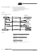
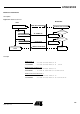
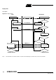
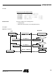

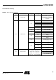

Table Of Contents
- Features
- Description
- Block Diagram
- SFR Mapping
- Pin Configurations
- Oscillators
- Enhanced Features
- Dual Data Pointer Register DPTR
- Expanded RAM (XRAM)
- Reset
- Power Monitor
- Timer 2
- Programmable Counter Array PCA
- Serial I/O Port
- Interrupt System
- Power Management
- Keyboard Interface
- 2-wire Interface (TWI)
- Serial Port Interface (SPI)
- Hardware Watchdog Timer
- ONCE(TM) Mode (ON Chip Emulation)
- Power-off Flag
- EEPROM Data Memory
- Reduced EMI Mode
- Flash Memory
- Electrical Characteristics
- Absolute Maximum Ratings
- DC Parameters
- AC Parameters
- Explanation of the AC Symbols
- External Program Memory Characteristics
- External Program Memory Read Cycle
- External Data Memory Characteristics
- External Data Memory Write Cycle
- External Data Memory Read Cycle
- Serial Port Timing - Shift Register Mode
- Shift Register Timing Waveforms
- External Clock Drive Waveforms
- AC Testing Input/Output Waveforms
- Float Waveforms
- Clock Waveforms
- Ordering Information
- Packaging Information
- Table of Contents

138
AT89C51ID2
4289C–8051–11/05
API Call Description Several Application Program Interface (API) calls are available for use by an application
program to permit selective erasing and programming of Flash pages. All calls are made
through a common interface, PGM_MTP. The programming functions are selected by
setting up the microcontroller’s registers before making a call to PGM_MTP at FFF0h.
Results are returned in the registers.
When several bytes have to be programmed, it is highly recommended to use the Atmel
API “PROGRAM DATA PAGE” call. Indeed, this API call writes up to 128 bytes in a sin-
gle command.
All routines for software access are provided in the C Flash driver available on Atmel
web site.
The API calls description and arguments are shown in Table
Table 97. API Call Summary
Command R1 A DPTR0 DPTR1 Returned Value Command Effect
READ MANUF ID 00h XXh 0000h XXh
ACC = Manufacturer
Id
Read Manufacturer identifier
READ DEVICE ID1 00h XXh 0001h XXh ACC = Device Id 1 Read Device identifier 1
READ DEVICE ID2 00h XXh 0002h XXh ACC = Device Id 2 Read Device identifier 2
READ DEVICE ID3 00h XXh 0003h XXh ACC = Device Id 3 Read Device identifier 3
ERASE BLOCK 01h XXh
DPH = 00h
00h ACC = DPH
Erase block 0
DPH = 20h Erase block 1
DPH = 40h Erase block 2
Address of
byte to
program
Program one Data Byte in user Flash
XXh
Erase Software boot vector and boot status
byte. (SBV = FCh and BSB = FFh)
PROGRAM SSB 05h XXh
DPH = 00h
DPL = 00h
00h ACC = SSB value
Set SSB level 1
DPH = 00h
DPL = 01h
Set SSB level 2
DPH = 00h
DPL = 10h
Set SSB level 0
DPH = 00h
DPL = 11h
Set SSB level 1
PROGRAM BSB 06h
New BSB
value
0000h XXh none Program boot status byte
PROGRAM SBV 06h
New SBV
value
0001h XXh none Program software boot vector
READ SSB 07h XXh 0000h XXh ACC = SSB Read Software Security Byte
READ BSB 07h XXh 0001h XXh ACC = BSB Read Boot Status Byte
READ SBV 07h XXh 0002h XXh ACC = SBV Read Software Boot Vector