
Datasheet
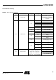
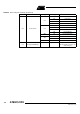

Table Of Contents
- Features
- Description
- Block Diagram
- SFR Mapping
- Pin Configurations
- Oscillators
- Enhanced Features
- Dual Data Pointer Register DPTR
- Expanded RAM (XRAM)
- Reset
- Power Monitor
- Timer 2
- Programmable Counter Array PCA
- Serial I/O Port
- Interrupt System
- Power Management
- Keyboard Interface
- 2-wire Interface (TWI)
- Serial Port Interface (SPI)
- Hardware Watchdog Timer
- ONCE(TM) Mode (ON Chip Emulation)
- Power-off Flag
- EEPROM Data Memory
- Reduced EMI Mode
- Flash Memory
- Electrical Characteristics
- Absolute Maximum Ratings
- DC Parameters
- AC Parameters
- Explanation of the AC Symbols
- External Program Memory Characteristics
- External Program Memory Read Cycle
- External Data Memory Characteristics
- External Data Memory Write Cycle
- External Data Memory Read Cycle
- Serial Port Timing - Shift Register Mode
- Shift Register Timing Waveforms
- External Clock Drive Waveforms
- AC Testing Input/Output Waveforms
- Float Waveforms
- Clock Waveforms
- Ordering Information
- Packaging Information
- Table of Contents
131
AT89C51ID2
4289C–8051–11/05
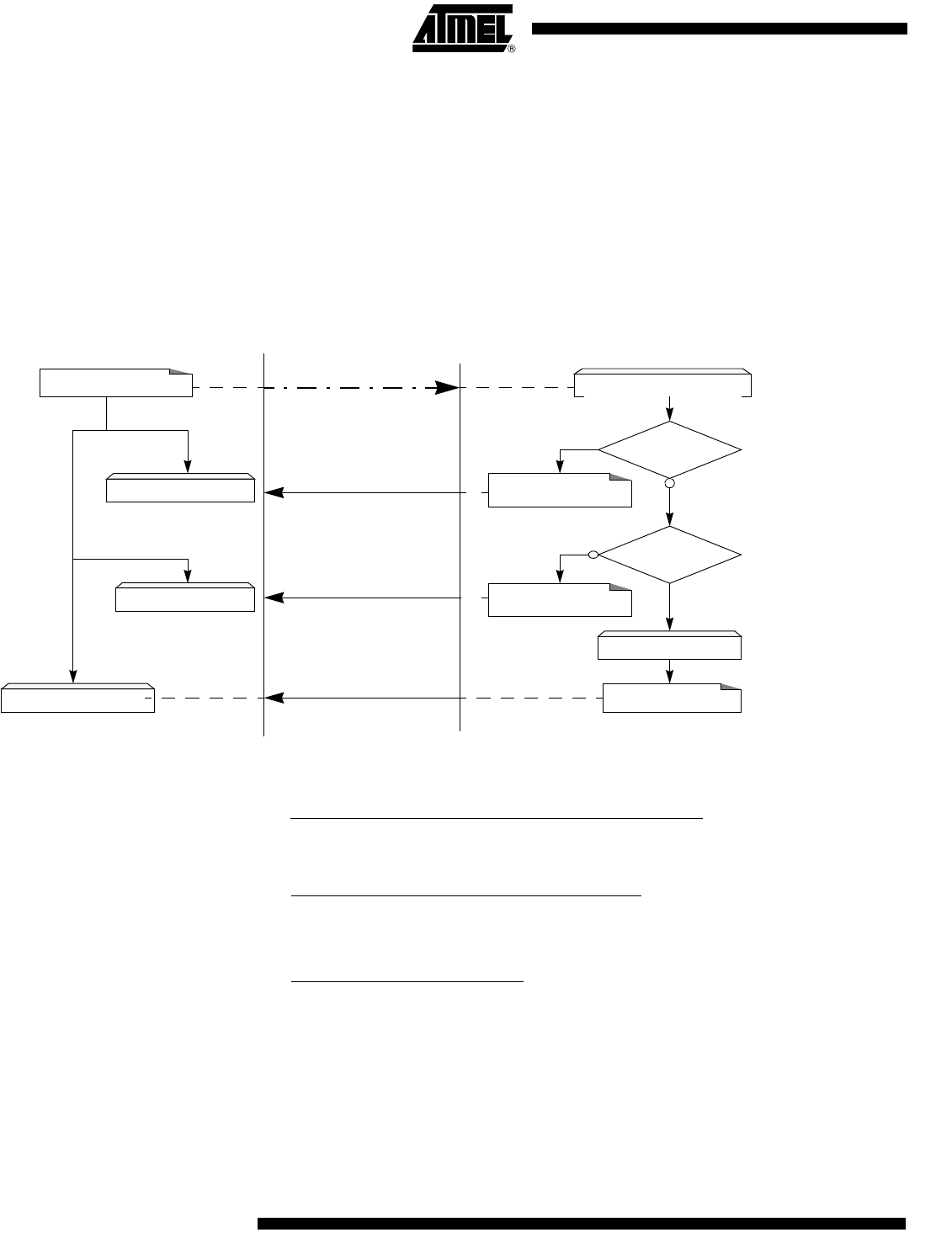
Write / Program Commands This flow is common to the following frames:
• Flash / Eeprom Programming Data Frame
• EOF or Atmel Frame (only Programming Atmel Frame)
• Config Byte Programming Data Frame
• Baud Rate Frame
Description
Figure 53. Write/Program Flow
Example
Host
Bootloader
Write Command
’X’ & CR & LF
NO_SECURITY
Wait Write Command
Checksum error
Wait Programming
Send Security error
Send COMMAND_OK
Send Write Command
Wait Checksum Error
Wait COMMAND_OK
Wait Security Error
OR
COMMAND ABORTED
COMMAND FINISHED
Send Checksum error
COMMAND ABORTED
’P’ & CR & LF
OR
’.’ & CR & LF
HOST : 01 0010 00 55 9A
BOOTLOADER : 01 0010 00 55 9A . CR LF
Programming Data (write 55h at address 0010h in the Flash)
HOST : 02 0000 03 05 01 F5
BOOTLOADER : 02 0000 03 05 01 F5. CR LF
Programming Atmel function (write SSB to level 2)
HOST : 03 0000 03 06 00 55 9F
BOOTLOADER
: 03 0000 03 06 00 55 9F . CR LF
Writing Frame (write BSB to 55h)