
Datasheet
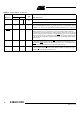
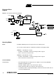
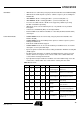
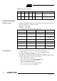
Table Of Contents
- Features
- Description
- Block Diagram
- SFR Mapping
- Pin Configurations
- Oscillators
- Enhanced Features
- Dual Data Pointer Register DPTR
- Expanded RAM (XRAM)
- Reset
- Power Monitor
- Timer 2
- Programmable Counter Array PCA
- Serial I/O Port
- Interrupt System
- Power Management
- Keyboard Interface
- 2-wire Interface (TWI)
- Serial Port Interface (SPI)
- Hardware Watchdog Timer
- ONCE(TM) Mode (ON Chip Emulation)
- Power-off Flag
- EEPROM Data Memory
- Reduced EMI Mode
- Flash Memory
- Electrical Characteristics
- Absolute Maximum Ratings
- DC Parameters
- AC Parameters
- Explanation of the AC Symbols
- External Program Memory Characteristics
- External Program Memory Read Cycle
- External Data Memory Characteristics
- External Data Memory Write Cycle
- External Data Memory Read Cycle
- Serial Port Timing - Shift Register Mode
- Shift Register Timing Waveforms
- External Clock Drive Waveforms
- AC Testing Input/Output Waveforms
- Float Waveforms
- Clock Waveforms
- Ordering Information
- Packaging Information
- Table of Contents
13
AT89C51ID2
4289C–8051–11/05
12 6 I/O
SDA (PI2.1): 2-wire Serial Data
SDA is the bidirectional 2-wire data line
RST 10 4 I
Reset: A high on this pin for two machine cycles while the oscillator is running, resets the
device. An internal diffused resistor to V
SS
permits a power-on reset using only an external
capacitor to V
CC
. This pin is an output when the hardware watchdog forces a system reset.
ALE/PROG
33 27 O (I) Address Latch Enable/Program Pulse: Output pulse for latching the low byte of the
address during an access to external memory. In normal operation, ALE is emitted at a
constant rate of 1/6 (1/3 in X2 mode) the oscillator frequency, and can be used for external
timing or clocking. Note that one ALE pulse is skipped during each access to external data
memory. This pin is also the program pulse input (PROG
) during Flash programming. ALE
can be disabled by setting SFR’s AUXR.0 bit. With this bit set, ALE will be inactive during
internal fetches.
PSEN 32 26 O Program Strobe ENable: The read strobe to external program memory. When executing
code from the external program memory, PSEN
is activated twice each machine cycle,
except that two PSEN
activations are skipped during each access to external data memory.
PSEN
is not activated during fetches from internal program memory.
EA 35 29 I External Access Enable: EA
must be externally held low to enable the device to fetch
code from external program memory locations 0000H to FFFFH. If security level 1 is pro-
grammed, EA
will be internally latched on Reset.
Table 15. Pin Description (Continued)
Mnemonic
Pin Number
Type
Name and FunctionPLCC44 VQFP44