
Datasheet
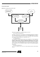
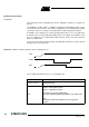
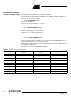
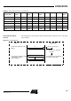
Table Of Contents
- Features
- Description
- Block Diagram
- SFR Mapping
- Pin Configurations
- Oscillators
- Enhanced Features
- Dual Data Pointer Register DPTR
- Expanded RAM (XRAM)
- Reset
- Power Monitor
- Timer 2
- Programmable Counter Array PCA
- Serial I/O Port
- Interrupt System
- Power Management
- Keyboard Interface
- 2-wire Interface (TWI)
- Serial Port Interface (SPI)
- Hardware Watchdog Timer
- ONCE(TM) Mode (ON Chip Emulation)
- Power-off Flag
- EEPROM Data Memory
- Reduced EMI Mode
- Flash Memory
- Electrical Characteristics
- Absolute Maximum Ratings
- DC Parameters
- AC Parameters
- Explanation of the AC Symbols
- External Program Memory Characteristics
- External Program Memory Read Cycle
- External Data Memory Characteristics
- External Data Memory Write Cycle
- External Data Memory Read Cycle
- Serial Port Timing - Shift Register Mode
- Shift Register Timing Waveforms
- External Clock Drive Waveforms
- AC Testing Input/Output Waveforms
- Float Waveforms
- Clock Waveforms
- Ordering Information
- Packaging Information
- Table of Contents

127
AT89C51ID2
4289C–8051–11/05
Functional Description
Software Security Bits (SSB) The SSB protects any Flash access from ISP command.
The command "Program Software Security bit" can only write a higher priority level.
There are three levels of security:
• level 0: NO_SECURITY (FFh)
This is the default level.
From level 0, one can write level 1 or level 2.
• level 1: WRITE_SECURITY (FEh )
For this level it is impossible to write in the Flash memory, BSB and SBV.
The Bootloader returns ’P’ on write access.
From level 1, one can write only level 2.
• level 2: RD_WR_SECURITY (FCh
The level 2 forbids all read and write accesses to/from the Flash/EEPROM memory.
The Bootloader returns ’L’ on read or write access.
Only a full chip erase in parallel mode (using a programmer) or ISP command can reset
the software security bits.
From level 2, one cannot read and write anything.
Table 94. Software Security Byte Behavior
Level 0 Level 1 Level 2
Flash/EEprom Any access allowed Read only access allowed Any access not allowed
Fuse bit Any access allowed Read only access allowed Any access not allowed
BSB & SBV Any access allowed Read only access allowed Any access not allowed
SSB Any access allowed Write level 2 allowed Read only access allowed
Manufacturer info Read only access allowed Read only access allowed Read only access allowed
Bootloader info Read only access allowed Read only access allowed Read only access allowed
Erase block Allowed Not allowed Not allowed
Full chip erase Allowed Allowed Allowed
Blank Check Allowed Allowed Allowed