
Datasheet
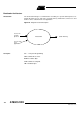


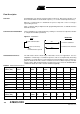
Table Of Contents
- Features
- Description
- Block Diagram
- SFR Mapping
- Pin Configurations
- Oscillators
- Enhanced Features
- Dual Data Pointer Register DPTR
- Expanded RAM (XRAM)
- Reset
- Power Monitor
- Timer 2
- Programmable Counter Array PCA
- Serial I/O Port
- Interrupt System
- Power Management
- Keyboard Interface
- 2-wire Interface (TWI)
- Serial Port Interface (SPI)
- Hardware Watchdog Timer
- ONCE(TM) Mode (ON Chip Emulation)
- Power-off Flag
- EEPROM Data Memory
- Reduced EMI Mode
- Flash Memory
- Electrical Characteristics
- Absolute Maximum Ratings
- DC Parameters
- AC Parameters
- Explanation of the AC Symbols
- External Program Memory Characteristics
- External Program Memory Read Cycle
- External Data Memory Characteristics
- External Data Memory Write Cycle
- External Data Memory Read Cycle
- Serial Port Timing - Shift Register Mode
- Shift Register Timing Waveforms
- External Clock Drive Waveforms
- AC Testing Input/Output Waveforms
- Float Waveforms
- Clock Waveforms
- Ordering Information
- Packaging Information
- Table of Contents
122
AT89C51ID2
4289C–8051–11/05
Functional Description
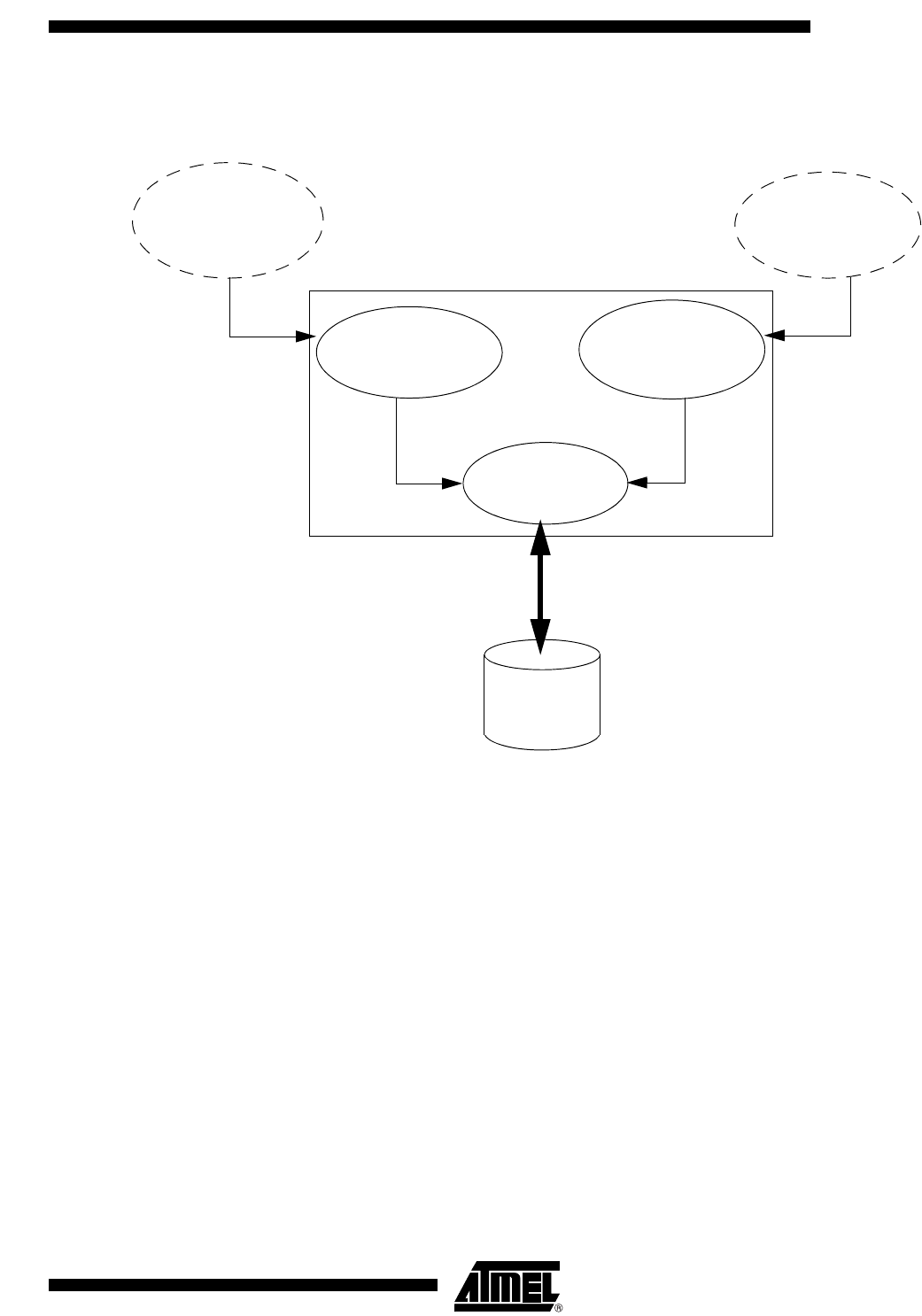
Figure 47. Bootloader Functional Description
On the above diagram, the on chip bootloader processes are:
• ISP Communication Management
The purpose of this process is to manage the communication and its protocol between
the on-chip bootloader and a external device. The on-chip ROM implement a serial pro-
tocol (see section Bootloader Protocol). This process translate serial communication
frame (UART) into flash memory acess (read, write, erase ...).
• User Call Management
Several Application Program Interface (API) calls are available for use by an application
program to permit selective erasing and programming of Flash pages. All calls are made
through a common interface (API calls), included in the ROM bootloader. The program-
ming functions are selected by setting up the microcontroller’s registers before making a
call to a common entry point (0xFFF0). Results are returned in the registers. The pur-
pose on this process is to translate the registers values into internal Flash Memory
Management.
• Flash Memory Management
This process manages low level access to flash memory (performs read and write
access).
ISP Communication
Management
User
Application
Specific Protocol
Communication
Management
Flash
Memory
Exernal host with
Flash Memory
User Call
Management (API )