
Datasheet
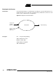
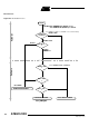

Table Of Contents
- Features
- Description
- Block Diagram
- SFR Mapping
- Pin Configurations
- Oscillators
- Enhanced Features
- Dual Data Pointer Register DPTR
- Expanded RAM (XRAM)
- Reset
- Power Monitor
- Timer 2
- Programmable Counter Array PCA
- Serial I/O Port
- Interrupt System
- Power Management
- Keyboard Interface
- 2-wire Interface (TWI)
- Serial Port Interface (SPI)
- Hardware Watchdog Timer
- ONCE(TM) Mode (ON Chip Emulation)
- Power-off Flag
- EEPROM Data Memory
- Reduced EMI Mode
- Flash Memory
- Electrical Characteristics
- Absolute Maximum Ratings
- DC Parameters
- AC Parameters
- Explanation of the AC Symbols
- External Program Memory Characteristics
- External Program Memory Read Cycle
- External Data Memory Characteristics
- External Data Memory Write Cycle
- External Data Memory Read Cycle
- Serial Port Timing - Shift Register Mode
- Shift Register Timing Waveforms
- External Clock Drive Waveforms
- AC Testing Input/Output Waveforms
- Float Waveforms
- Clock Waveforms
- Ordering Information
- Packaging Information
- Table of Contents

121
AT89C51ID2
4289C–8051–11/05
Bootloader Architecture
Introduction The bootloader manages a communication according to a specific defined protocol to
provide the whole access and service on Flash memory. Furthermore, all accesses and
routines can be called from the user application.
Figure 46. Diagram Context Description
Acronyms ISP : In-System Programming
SBV: Software Boot Vector
BSB: Boot Status Byte
SSB: Software Security Bit
HW : Hardware Byte
Bootloader
Flash memory
access via
specific
protocol
access from
user
application