
Datasheet
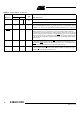
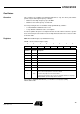
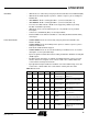
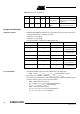
Table Of Contents
- Features
- Description
- Block Diagram
- SFR Mapping
- Pin Configurations
- Oscillators
- Enhanced Features
- Dual Data Pointer Register DPTR
- Expanded RAM (XRAM)
- Reset
- Power Monitor
- Timer 2
- Programmable Counter Array PCA
- Serial I/O Port
- Interrupt System
- Power Management
- Keyboard Interface
- 2-wire Interface (TWI)
- Serial Port Interface (SPI)
- Hardware Watchdog Timer
- ONCE(TM) Mode (ON Chip Emulation)
- Power-off Flag
- EEPROM Data Memory
- Reduced EMI Mode
- Flash Memory
- Electrical Characteristics
- Absolute Maximum Ratings
- DC Parameters
- AC Parameters
- Explanation of the AC Symbols
- External Program Memory Characteristics
- External Program Memory Read Cycle
- External Data Memory Characteristics
- External Data Memory Write Cycle
- External Data Memory Read Cycle
- Serial Port Timing - Shift Register Mode
- Shift Register Timing Waveforms
- External Clock Drive Waveforms
- AC Testing Input/Output Waveforms
- Float Waveforms
- Clock Waveforms
- Ordering Information
- Packaging Information
- Table of Contents
12
AT89C51ID2
4289C–8051–11/05
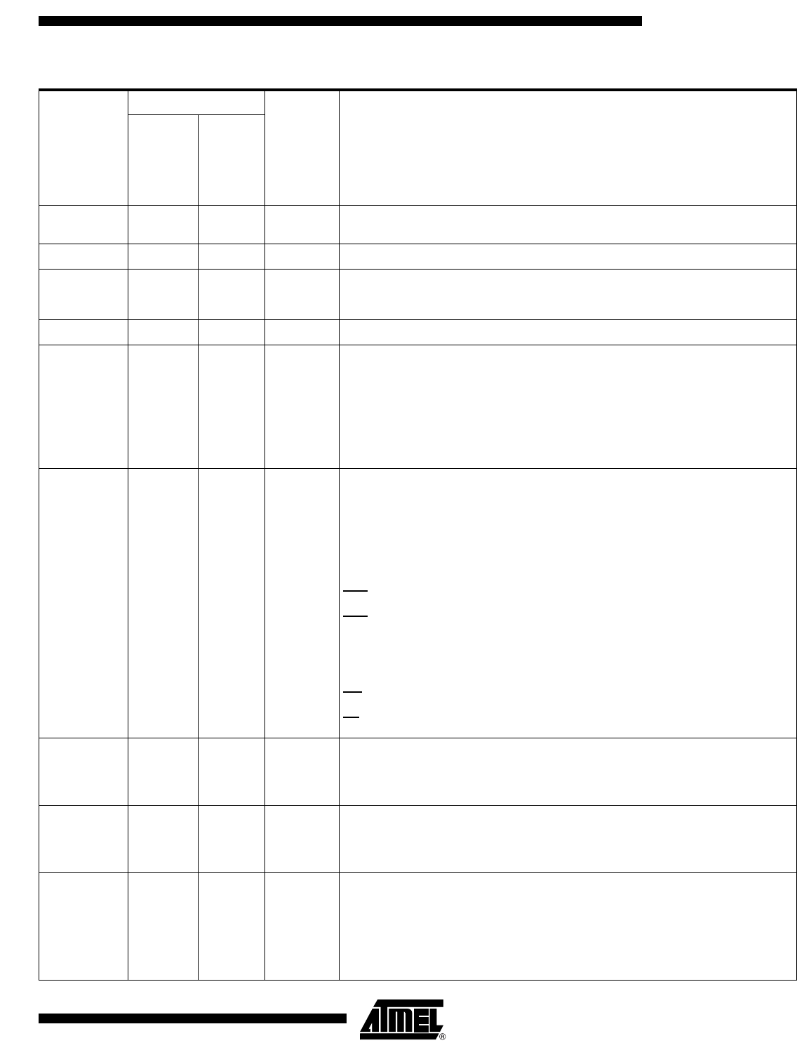
I/O MOSI: SPI Master Output Slave Input line
When SPI is in master mode, MOSI outputs data to the slave peripheral. When SPI is in
slave mode, MOSI receives data from the master controller.
XTALA1 21 15 I
Crystal A 1: Input to the inverting oscillator amplifier and input to the internal clock genera-
tor circuits.
XTALA2 20 14 O Crystal A 2: Output from the inverting oscillator amplifier
XTALB1 2 40 I
Crystal B 1: (Sub Clock) Input to the inverting oscillator amplifier and input to the internal
clock generator circuits.
XTALB2 1 39 O Crystal B 2: (Sub Clock) Output from the inverting oscillator amplifier
P2.0 - P2.7 24 - 31 18 - 25
I/O
Port 2: Port 2 is an 8-bit bidirectional I/O port with internal pull-ups. Port 2 pins that have 1s
written to them are pulled high by the internal pull-ups and can be used as inputs. As
inputs, Port 2 pins that are externally pulled low will source current because of the internal
pull-ups. Port 2 emits the high-order address byte during fetches from external program
memory and during accesses to external data memory that use 16-bit addresses (MOVX
@DPTR).In this application, it uses strong internal pull-ups emitting 1s. During accesses to
external data memory that use 8-bit addresses (MOVX @Ri), port 2 emits the contents of
the P2 SFR.
P3.0 - P3.7 11,
13 - 19
5,
7 - 13
I/O Port 3: Port 3 is an 8-bit bidirectional I/O port with internal pull-ups. Port 3 pins that have 1s
written to them are pulled high by the internal pull-ups and can be used as inputs. As
inputs, Port 3 pins that are externally pulled low will source current because of the internal
pull-ups. Port 3 also serves the special features of the 80C51 family, as listed below.
11 5 I RXD (P3.0): Serial input port
13 7 O TXD (P3.1): Serial output port
14 8 I INT0
(P3.2): External interrupt 0
15 9 I INT1
(P3.3): External interrupt 1
16 10 I T0 (P3.4): Timer 0 external input
17 11 I T1 (P3.5): Timer 1 external input
18 12 O WR
(P3.6): External data memory write strobe
19 13 O RD
(P3.7): External data memory read strobe
P4.0 - P4.7
- - I/O
Port 4: Port 4 is an 8-bit bidirectional I/O port with internal pull-ups. Port 5 pins that have 1s
written to them are pulled high by the internal pull-ups and can be used as inputs. As
inputs, Port 4 pins that are externally pulled low will source current because of the internal
pull-ups.
P5.0 - P5.7
- - I/O
Port 5: Port 5 is an 8-bit bidirectional I/O port with internal pull-ups. Port 3 pins that have 1s
written to them are pulled high by the internal pull-ups and can be used as inputs. As
inputs, Port 5 pins that are externally pulled low will source current because of the internal
pull-ups.
PI2.0 - PI2.1
34, 12 28, 6
Port I2: Port I2 is an open drain. It can be used as inputs (must be polarized to Vcc with
external resistor to prevent any parasitic current consumption).
34 28 I/O SCL (PI2.0): 2-wire Serial Clock
SCL output the serial clock to slave peripherals
SCL input the serial clock from master
Table 15. Pin Description (Continued)
Mnemonic
Pin Number
Type
Name and FunctionPLCC44 VQFP44