
Datasheet
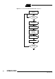
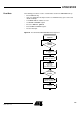
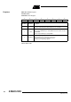
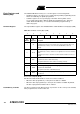
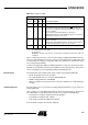
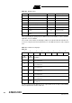
Table Of Contents
- Features
- Description
- Block Diagram
- SFR Mapping
- Pin Configurations
- Oscillators
- Enhanced Features
- Dual Data Pointer Register DPTR
- Expanded RAM (XRAM)
- Reset
- Power Monitor
- Timer 2
- Programmable Counter Array PCA
- Serial I/O Port
- Interrupt System
- Power Management
- Keyboard Interface
- 2-wire Interface (TWI)
- Serial Port Interface (SPI)
- Hardware Watchdog Timer
- ONCE(TM) Mode (ON Chip Emulation)
- Power-off Flag
- EEPROM Data Memory
- Reduced EMI Mode
- Flash Memory
- Electrical Characteristics
- Absolute Maximum Ratings
- DC Parameters
- AC Parameters
- Explanation of the AC Symbols
- External Program Memory Characteristics
- External Program Memory Read Cycle
- External Data Memory Characteristics
- External Data Memory Write Cycle
- External Data Memory Read Cycle
- Serial Port Timing - Shift Register Mode
- Shift Register Timing Waveforms
- External Clock Drive Waveforms
- AC Testing Input/Output Waveforms
- Float Waveforms
- Clock Waveforms
- Ordering Information
- Packaging Information
- Table of Contents
119
AT89C51ID2
4289C–8051–11/05
Table 90. Default Values
After programming the part by ISP, the BSB must be cleared (00h) in order to allow the
application to boot at 0000h.
The content of the Software Security Byte (SSB) is described in Table 90 and Table 93.
To assure code protection from a parallel access, the HSB must also be at the required
level.
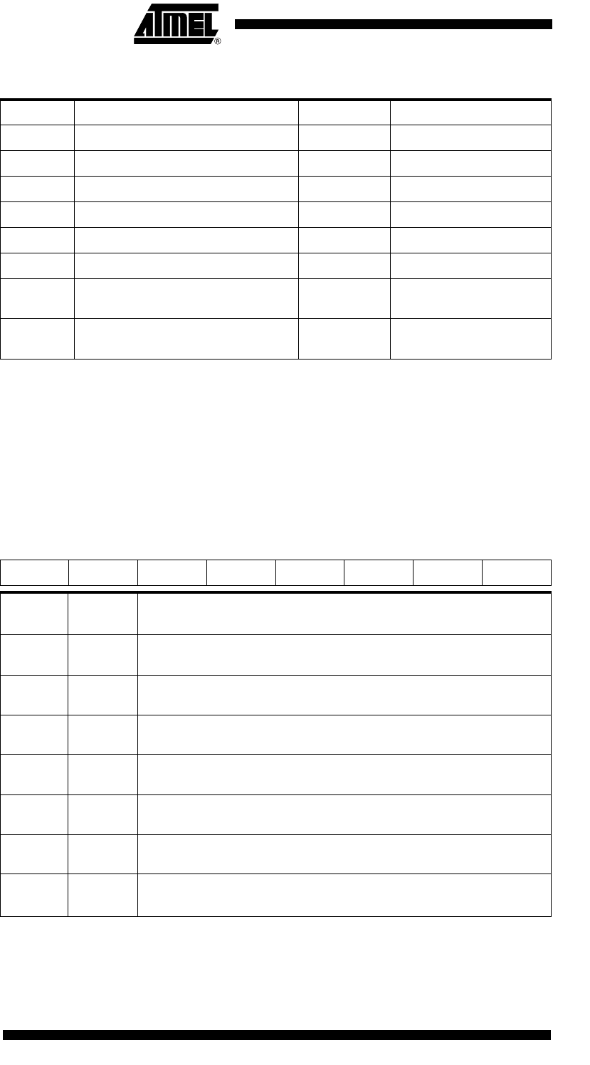
Table 91. Software Security Byte
The two lock bits provide different levels of protection for the on-chip code and data,
when programmed as shown to Table 93.
Mnemonic Definition Default value Description
SBV Software Boot Vector FCh
HSB Copy of the Hardware security byte 101x 1011b
BSB Boot Status Byte 0FFh
SSB Software Security Byte FFh
Copy of the Manufacturer Code 58h ATMEL
Copy of the Device ID #1: Family Code D7h C51 X2, Electrically Erasable
Copy of the Device ID #2: memories size
and type
ECh AT89C51ID2 64KB
Copy of the Device ID #3: name and
revision
EFh
AT89C51ID2 64KB, Revision
0
Table 92.
76543210
------LB1LB0
Bit
Number
Bit
Mnemonic Description
7-
Reserved
Do not clear this bit.
6-
Reserved
Do not clear this bit.
5-
Reserved
Do not clear this bit.
4-
Reserved
Do not clear this bit.
3-
Reserved
Do not clear this bit.
2-
Reserved
Do not clear this bit.
1-0 LB1-0
User Memory Lock Bits
See Table 93