
Datasheet
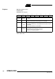
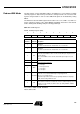
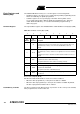
Table Of Contents
- Features
- Description
- Block Diagram
- SFR Mapping
- Pin Configurations
- Oscillators
- Enhanced Features
- Dual Data Pointer Register DPTR
- Expanded RAM (XRAM)
- Reset
- Power Monitor
- Timer 2
- Programmable Counter Array PCA
- Serial I/O Port
- Interrupt System
- Power Management
- Keyboard Interface
- 2-wire Interface (TWI)
- Serial Port Interface (SPI)
- Hardware Watchdog Timer
- ONCE(TM) Mode (ON Chip Emulation)
- Power-off Flag
- EEPROM Data Memory
- Reduced EMI Mode
- Flash Memory
- Electrical Characteristics
- Absolute Maximum Ratings
- DC Parameters
- AC Parameters
- Explanation of the AC Symbols
- External Program Memory Characteristics
- External Program Memory Read Cycle
- External Data Memory Characteristics
- External Data Memory Write Cycle
- External Data Memory Read Cycle
- Serial Port Timing - Shift Register Mode
- Shift Register Timing Waveforms
- External Clock Drive Waveforms
- AC Testing Input/Output Waveforms
- Float Waveforms
- Clock Waveforms
- Ordering Information
- Packaging Information
- Table of Contents
118
AT89C51ID2
4289C–8051–11/05
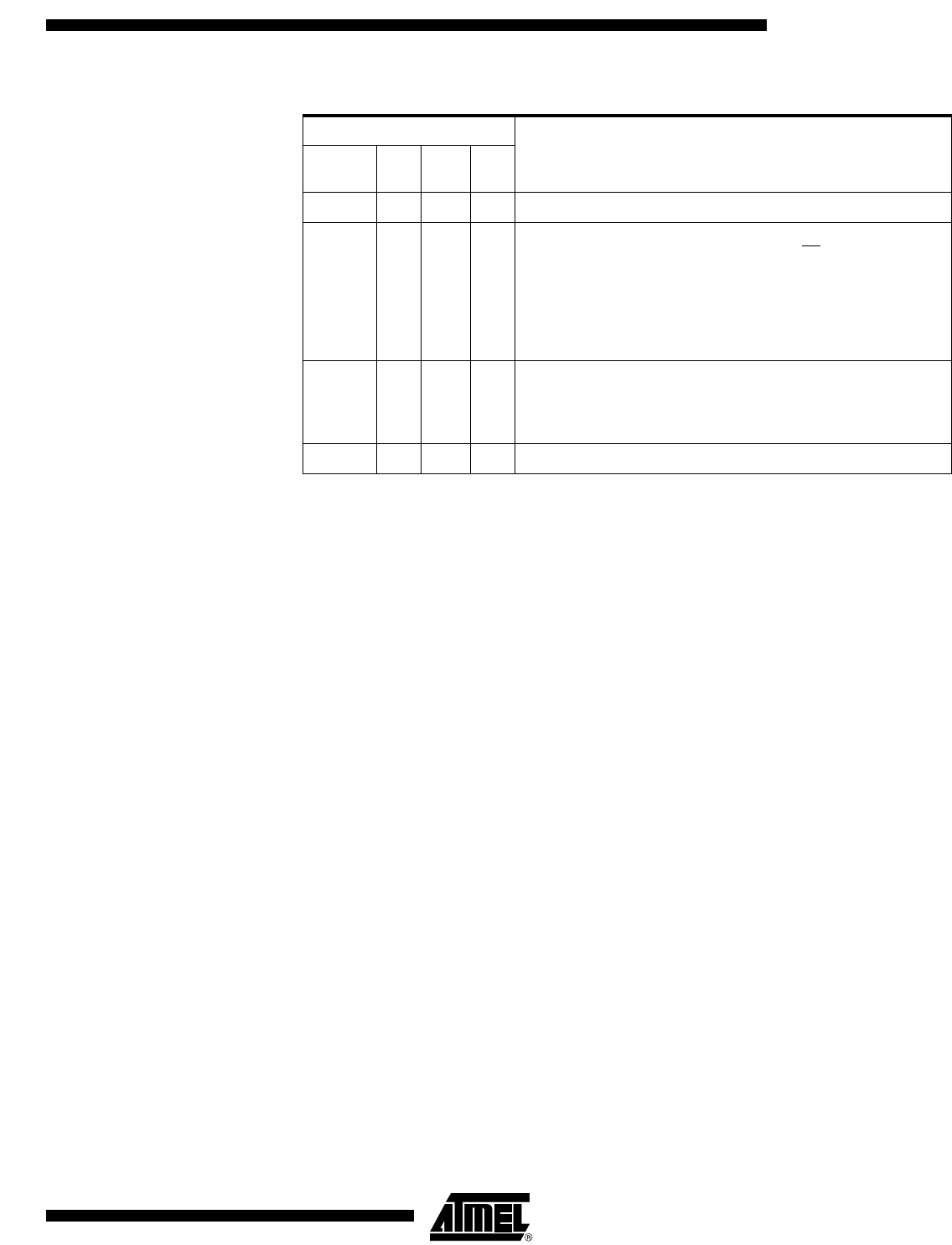
Table 89. Program Lock Bits
Note: U: unprogrammed or "one" level.
P: programmed or "zero" level.
X: do not care
WARNING: Security level 2 and 3 should only be programmed after Flash and code
verification.
These security bits protect the code access through the parallel programming interface.
They are set by default to level 4. The code access through the ISP is still possible and
is controlled by the "software security bits" which are stored in the extra Flash memory
accessed by the ISP firmware.
To load a new application with the parallel programmer, a chip erase must first be done.
This will set the HSB in its inactive state and will erase the Flash memory. The part ref-
erence can always be read using Flash parallel programming modes.
Default Values The default value of the HSB provides parts ready to be programmed with ISP:
• BLJB: Programmed force ISP operation.
• X2: Unprogrammed to force X1 mode (Standard Mode).
• XRAM: Unprogrammed to valid XRAM
• LB2-0: Security level four to protect the code from a parallel access with maximum
security.
Software Registers Several registers are used, in factory and by parallel programmers. These values are
used by Atmel ISP.
These registers are in the "Extra Flash Memory" part of the Flash memory. This block is
also called "XAF" or eXtra Array Flash. They are accessed in the following ways:
• Commands issued by the parallel memory programmer.
• Commands issued by the ISP software.
• Calls of API issued by the application software.
Several software registers described in Table 90.
Program Lock Bits
Protection description
Security
level LB0 LB1 LB2
1 U U U No program lock features enabled.
2PUU
MOVC instruction executed from external program memory is disabled
from fetching code bytes from internal memory, EA
is sampled and
latched on reset, and further parallel programming of the on chip code
memory is disabled.
ISP and software programming with API are still allowed.
Writing EEprom Data from external parallel programmer is disabled but
still allowed from internal code execution.
3XPU
Same as 2, also verify code memory through parallel programming
interface is disabled.
Writing And Reading EEPROM Data from external parallel programmer
is disabled but still allowed from internal code execution..
4 X X P Same as 3, also external execution is disabled. (Default)