
Datasheet
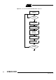
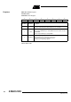
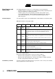
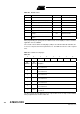
Table Of Contents
- Features
- Description
- Block Diagram
- SFR Mapping
- Pin Configurations
- Oscillators
- Enhanced Features
- Dual Data Pointer Register DPTR
- Expanded RAM (XRAM)
- Reset
- Power Monitor
- Timer 2
- Programmable Counter Array PCA
- Serial I/O Port
- Interrupt System
- Power Management
- Keyboard Interface
- 2-wire Interface (TWI)
- Serial Port Interface (SPI)
- Hardware Watchdog Timer
- ONCE(TM) Mode (ON Chip Emulation)
- Power-off Flag
- EEPROM Data Memory
- Reduced EMI Mode
- Flash Memory
- Electrical Characteristics
- Absolute Maximum Ratings
- DC Parameters
- AC Parameters
- Explanation of the AC Symbols
- External Program Memory Characteristics
- External Program Memory Read Cycle
- External Data Memory Characteristics
- External Data Memory Write Cycle
- External Data Memory Read Cycle
- Serial Port Timing - Shift Register Mode
- Shift Register Timing Waveforms
- External Clock Drive Waveforms
- AC Testing Input/Output Waveforms
- Float Waveforms
- Clock Waveforms
- Ordering Information
- Packaging Information
- Table of Contents

117
AT89C51ID2
4289C–8051–11/05
Flash Registers and
Memory Map
The AT89C51ID2 Flash memory uses several registers for his management:
• Hardware registers can only be accessed through the parallel programming modes
which are handled by the parallel programmer.
• Software registers are in a special page of the Flash memory which can be
accessed through the API or with the parallel programming modes. This page,
called "Extra Flash Memory", is not in the internal Flash program memory
addressing space.
Hardware Register The only hardware register of the AT89C51ID2 is called Hardware Security Byte (HSB).
Table 88. Hardware Security Byte (HSB)
Boot Loader Jump Bit (BLJB)
One bit of the HSB, the BLJB bit, is used to force the boot address:
• When this bit is programmed (‘1’ value) the boot address is 0000h.
• When this bit is unprogrammed (‘1’ value) the boot address is F800h. By default,
this bit is unprogrammed and the ISP is enabled.
Flash Memory Lock Bits The three lock bits provide different levels of protection for the on-chip code and data,
when programmed as shown in Table 89.
76543210
X2 BLJB OSC - XRAM LB2 LB1 LB0
Bit
Number
Bit
Mnemonic Description
7X2
X2 Mode
Programmed (‘0’ value) to force X2 mode (6 clocks per instruction) after reset.
Unprogrammed (‘1’ Value) to force X1 mode, Standard Mode, after reset
(Default).
6BLJB
Boot Loader Jump Bit
Unprogrammed (‘1’ value) to start the user’s application on next reset at address
0000h.
Programmed (‘0’ value) to start the boot loader at address F800h on next reset
(Default).
5OSC
Oscillator Bit
Programmed to allow oscillator B at startup
Unprogrammed this bit to allow oscillator A at startup ( Default).
4-
Reserved
3XRAM
XRAM config bit (only programmable by programmer tools)
Programmed to inhibit XRAM
Unprogrammed, this bit to valid XRAM (Default)
2-0 LB2-0
User Memory Lock Bits (only programmable by programmer tools)
See Table 89