
Datasheet
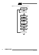
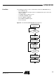
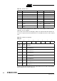
Table Of Contents
- Features
- Description
- Block Diagram
- SFR Mapping
- Pin Configurations
- Oscillators
- Enhanced Features
- Dual Data Pointer Register DPTR
- Expanded RAM (XRAM)
- Reset
- Power Monitor
- Timer 2
- Programmable Counter Array PCA
- Serial I/O Port
- Interrupt System
- Power Management
- Keyboard Interface
- 2-wire Interface (TWI)
- Serial Port Interface (SPI)
- Hardware Watchdog Timer
- ONCE(TM) Mode (ON Chip Emulation)
- Power-off Flag
- EEPROM Data Memory
- Reduced EMI Mode
- Flash Memory
- Electrical Characteristics
- Absolute Maximum Ratings
- DC Parameters
- AC Parameters
- Explanation of the AC Symbols
- External Program Memory Characteristics
- External Program Memory Read Cycle
- External Data Memory Characteristics
- External Data Memory Write Cycle
- External Data Memory Read Cycle
- Serial Port Timing - Shift Register Mode
- Shift Register Timing Waveforms
- External Clock Drive Waveforms
- AC Testing Input/Output Waveforms
- Float Waveforms
- Clock Waveforms
- Ordering Information
- Packaging Information
- Table of Contents

116
AT89C51ID2
4289C–8051–11/05
Flash Memory The Flash memory increases EPROM and ROM functionality with in-circuit electrical
erasure and programming. It contains 64K bytes of program memory organized respec-
tively in 512 pages of 128 bytes. This memory is both parallel and serial In-System
Programmable (ISP). ISP allows devices to alter their own program memory in the
actual end product under software control. A default serial loader (bootloader) program
allows ISP of the Flash.
The programming does not require external dedicated programming voltage. The nec-
essary high programming voltage is generated on-chip using the standard V
CC
pins of
the microcontroller.
Features • Flash internal program memory.
• Boot vector allows user provided Flash loader code to reside anywhere in the Flash
memory space. This configuration provides flexibility to the user.
• Default loader in Boot ROM allows programming via the serial port without the need
of a user provided loader.
• Up to 64K byte external program memory if the internal program memory is disabled
(EA = 0).
• Programming and erase voltage with standard power supply.
• Read/Programming/Erase:
• Byte-wise read without wait state
• Byte or page erase and programming (10 ms)
• Typical programming time (64K bytes) is 22s with on chip serial bootloader
• Parallel programming with 87C51 compatible hardware interface to programmer
• Programmable security for the code in the Flash
• 100k write cycles
• 10 years data retention
Flash Programming and
Erasure
The 64K bytes Flash is programmed by bytes or by pages of 128 bytes. It is not neces-
sary to erase a byte or a page before programming. The programming of a byte or a
page includes a self erase before programming.
There are three methods of programming the Flash memory:
• First, the on-chip ISP bootloader may be invoked which will use low level routines to
program the pages. The interface used for serial downloading of Flash is the UART.
• Second, the Flash may be programmed or erased in the end-user application by
calling low-level routines through a common entry point in the Boot ROM.
• Third, the Flash may be programmed using the parallel method by using a
conventional EPROM programmer. The parallel programming method used by
these devices is similar to that used by EPROM 87C51 but it is not identical and the
commercially available programmers need to have support for the AT89C51ID2.
The bootloader and the Application Programming Interface (API) routines are
located in the BOOT ROM.