
Datasheet
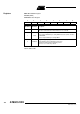
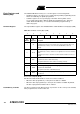
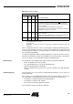
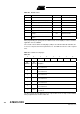
Table Of Contents
- Features
- Description
- Block Diagram
- SFR Mapping
- Pin Configurations
- Oscillators
- Enhanced Features
- Dual Data Pointer Register DPTR
- Expanded RAM (XRAM)
- Reset
- Power Monitor
- Timer 2
- Programmable Counter Array PCA
- Serial I/O Port
- Interrupt System
- Power Management
- Keyboard Interface
- 2-wire Interface (TWI)
- Serial Port Interface (SPI)
- Hardware Watchdog Timer
- ONCE(TM) Mode (ON Chip Emulation)
- Power-off Flag
- EEPROM Data Memory
- Reduced EMI Mode
- Flash Memory
- Electrical Characteristics
- Absolute Maximum Ratings
- DC Parameters
- AC Parameters
- Explanation of the AC Symbols
- External Program Memory Characteristics
- External Program Memory Read Cycle
- External Data Memory Characteristics
- External Data Memory Write Cycle
- External Data Memory Read Cycle
- Serial Port Timing - Shift Register Mode
- Shift Register Timing Waveforms
- External Clock Drive Waveforms
- AC Testing Input/Output Waveforms
- Float Waveforms
- Clock Waveforms
- Ordering Information
- Packaging Information
- Table of Contents

115
AT89C51ID2
4289C–8051–11/05
Reduced EMI Mode The ALE signal is used to demultiplex address and data buses on port 0 when used with
external program or data memory. Nevertheless, during internal code execution, ALE
signal is still generated. In order to reduce EMI, ALE signal can be disabled by setting
AO bit.
The AO bit is located in AUXR register at bit location 0. As soon as AO is set, ALE is no
longer output but remains active during MOVX and MOVC instructions and external
fetches. During ALE disabling, ALE pin is weakly pulled high.
Table 87. AUXR Register
AUXR - Auxiliary Register (8Eh)
Reset Value = XX00 10’HSB. XRAM’0b
Not bit addressable
76543210
- - M0 XRS2 XRS1 XRS0 EXTRAM AO
Bit
Number
Bit
Mnemonic Description
7-
Reserved
The value read from this bit is indeterminate. Do not set this bit.
6-
Reserved
The value read from this bit is indeterminate. Do not set this bit.
5M0
Pulse length
Cleared to stretch MOVX control: the RD/ and the WR/ pulse length is 6 clock
periods (default).
Set to stretch MOVX control: the RD/ and the WR/ pulse length is 30 clock
periods.
4XRS2
XRAM Size
XRS2 XRS1XRS0XRAM size
0 0 0 256 bytes
0 0 1 512 bytes
0 1 0 768 bytes(default)
0 1 1 1024 bytes
1 0 0 1792 bytes
3XRS1
2XRS0
1 EXTRAM
EXTRAM bit
Cleared to access internal XRAM using movx @ Ri/ @ DPTR.
Set to access external memory.
Programmed by hardware after Power-up regarding Hardware Security Byte
(HSB), default setting, XRAM selected.
0AO
ALE Output bit
Cleared, ALE is emitted at a constant rate of 1/6 the oscillator frequency (or 1/3 if
X2 mode is used). (default) Set, ALE is active only during a MOVX or MOVC
instruction is used.