
Datasheet
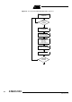
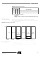
Table Of Contents
- Features
- Description
- Block Diagram
- SFR Mapping
- Pin Configurations
- Oscillators
- Enhanced Features
- Dual Data Pointer Register DPTR
- Expanded RAM (XRAM)
- Reset
- Power Monitor
- Timer 2
- Programmable Counter Array PCA
- Serial I/O Port
- Interrupt System
- Power Management
- Keyboard Interface
- 2-wire Interface (TWI)
- Serial Port Interface (SPI)
- Hardware Watchdog Timer
- ONCE(TM) Mode (ON Chip Emulation)
- Power-off Flag
- EEPROM Data Memory
- Reduced EMI Mode
- Flash Memory
- Electrical Characteristics
- Absolute Maximum Ratings
- DC Parameters
- AC Parameters
- Explanation of the AC Symbols
- External Program Memory Characteristics
- External Program Memory Read Cycle
- External Data Memory Characteristics
- External Data Memory Write Cycle
- External Data Memory Read Cycle
- Serial Port Timing - Shift Register Mode
- Shift Register Timing Waveforms
- External Clock Drive Waveforms
- AC Testing Input/Output Waveforms
- Float Waveforms
- Clock Waveforms
- Ordering Information
- Packaging Information
- Table of Contents

111
AT89C51ID2
4289C–8051–11/05
EEPROM Data
Memory
The 2K bytes on-chip EEPROM memory block is located at addresses 0000h to 07FFh
of the XRAM/ERAM memory space and is selected by setting control bits in the EECON
register.
A read or write access to the EEPROM memory is done with a MOVX instruction.
Write Data Data is written by byte to the EEPROM memory block as for an external RAM memory.
The following procedure is used to write to the EEPROM memory:
• Check EEBUSY flag
• If the user application interrupts routines use XRAM memory space: Save and
disable interrupts.
• Load DPTR with the address to write
• Store A register with the data to be written
• Set bit EEE of EECON register
• Execute a MOVX @DPTR, A
• Clear bit EEE of EECON register
• Restore interrupts.
• EEBUSY flag in EECON is then set by hardware to indicate that programming is in
progress and that the EEPROM segment is not available for reading or writing.
• The end of programming is indicated by a hardware clear of the EEBUSY flag.
Figure 43 represents the optimal write sequence to the on-chip EEPROM data memory.