
Datasheet

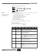

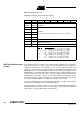

Table Of Contents
- Features
- Description
- Block Diagram
- SFR Mapping
- Pin Configurations
- Oscillators
- Enhanced Features
- Dual Data Pointer Register DPTR
- Expanded RAM (XRAM)
- Reset
- Power Monitor
- Timer 2
- Programmable Counter Array PCA
- Serial I/O Port
- Interrupt System
- Power Management
- Keyboard Interface
- 2-wire Interface (TWI)
- Serial Port Interface (SPI)
- Hardware Watchdog Timer
- ONCE(TM) Mode (ON Chip Emulation)
- Power-off Flag
- EEPROM Data Memory
- Reduced EMI Mode
- Flash Memory
- Electrical Characteristics
- Absolute Maximum Ratings
- DC Parameters
- AC Parameters
- Explanation of the AC Symbols
- External Program Memory Characteristics
- External Program Memory Read Cycle
- External Data Memory Characteristics
- External Data Memory Write Cycle
- External Data Memory Read Cycle
- Serial Port Timing - Shift Register Mode
- Shift Register Timing Waveforms
- External Clock Drive Waveforms
- AC Testing Input/Output Waveforms
- Float Waveforms
- Clock Waveforms
- Ordering Information
- Packaging Information
- Table of Contents

109
AT89C51ID2
4289C–8051–11/05
ONCE
(TM)
Mode (ON
Chip Emulation)
The ONCE mode facilitates testing and debugging of systems using AT89C51ID2 with-
out removing the circuit from the board. The ONCE mode is invoked by driving certain
pins of the AT89C51ID2; the following sequence must be exercised:
• Pull ALE low while the device is in reset (RST high) and PSEN
is high.
• Hold ALE low as RST is deactivated.
While the AT89C51ID2 is in ONCE mode, an emulator or test CPU can be used to drive
the circuit Table 84 shows the status of the port pins during ONCE mode.
Normal operation is restored when normal reset is applied.
Table 84. External Pin Status during ONCE Mode
(a) "Once" is a registered trademark of Intel Corporation.
ALE PSEN Port 0 Port 1 Port 2 Port 3 Port I2 XTALA1/2 XTALB1/2
Weak
pull-up
Weak
pull-up
Float
Weak
pull-up
Weak
pull-up
Weak
pull-up
Float Active Active