
Datasheet

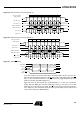


Table Of Contents
- Features
- Description
- Block Diagram
- SFR Mapping
- Pin Configurations
- Oscillators
- Enhanced Features
- Dual Data Pointer Register DPTR
- Expanded RAM (XRAM)
- Reset
- Power Monitor
- Timer 2
- Programmable Counter Array PCA
- Serial I/O Port
- Interrupt System
- Power Management
- Keyboard Interface
- 2-wire Interface (TWI)
- Serial Port Interface (SPI)
- Hardware Watchdog Timer
- ONCE(TM) Mode (ON Chip Emulation)
- Power-off Flag
- EEPROM Data Memory
- Reduced EMI Mode
- Flash Memory
- Electrical Characteristics
- Absolute Maximum Ratings
- DC Parameters
- AC Parameters
- Explanation of the AC Symbols
- External Program Memory Characteristics
- External Program Memory Read Cycle
- External Data Memory Characteristics
- External Data Memory Write Cycle
- External Data Memory Read Cycle
- Serial Port Timing - Shift Register Mode
- Shift Register Timing Waveforms
- External Clock Drive Waveforms
- AC Testing Input/Output Waveforms
- Float Waveforms
- Clock Waveforms
- Ordering Information
- Packaging Information
- Table of Contents
105
AT89C51ID2
4289C–8051–11/05
Reset Value = 0001 0100b
Not bit addressable
Serial Peripheral Status Register
(SPSTA)
The Serial Peripheral Status Register contains flags to signal the following conditions:
• Data transfer complete
• Write collision
• Inconsistent logic level on SS
pin (mode fault error)
Table 80 describes the SPSTA register and explains the use of every bit in the register.
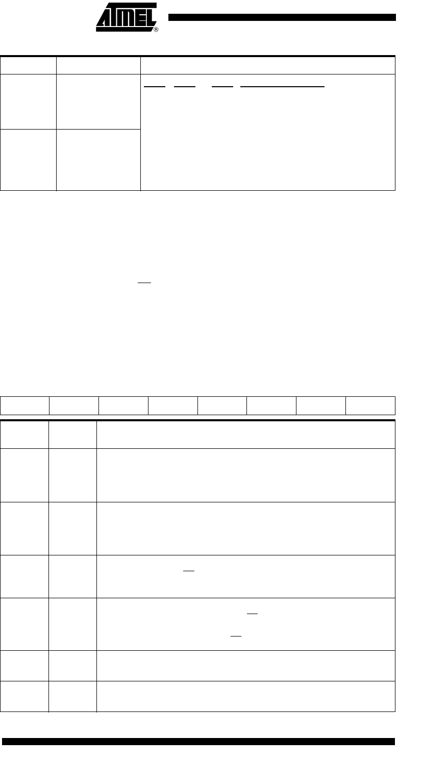
Table 80. SPSTA Register
SPSTA - Serial Peripheral Status and Control register (0C4H)
1
SPR1
SPR2 SPR1 SPR0 Serial Peripheral Rate
00 0F
CLK PERIPH
/2
00 1 F
CLK PERIPH
/4
01 0 F
CLK PERIPH
/8
01 1F
CLK PERIPH
/16
10 0F
CLK PERIPH
/32
10 1F
CLK PERIPH
/64
11 0F
CLK PERIPH
/128
1 1 1 Invalid
0 SPR0
Bit Number Bit Mnemonic Description
Table 2.
76543210
SPIF WCOL SSERR MODF - - - -
Bit
Number
Bit
Mnemonic Description
7SPIF
Serial Peripheral Data Transfer Flag
Cleared by hardware to indicate data transfer is in progress or has been
approved by a clearing sequence.
Set by hardware to indicate that the data transfer has been completed.
6WCOL
Write Collision Flag
Cleared by hardware to indicate that no collision has occurred or has been
approved by a clearing sequence.
Set by hardware to indicate that a collision has been detected.
5 SSERR
Synchronous Serial Slave Error Flag
Set by hardware when SS is deasserted before the end of a received data.
Cleared by disabling the SPI (clearing SPEN bit in SPCON).
4MODF
Mode Fault
Cleared by hardware to indicate that the SS pin is at appropriate logic level, or
has been approved by a clearing sequence.
Set by hardware to indicate that the SS
pin is at inappropriate logic level.
3-
Reserved
The value read from this bit is indeterminate. Do not set this bit
2-
Reserved
The value read from this bit is indeterminate. Do not set this bit.