
Datasheet

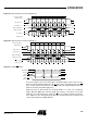
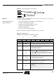
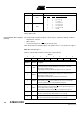


Table Of Contents
- Features
- Description
- Block Diagram
- SFR Mapping
- Pin Configurations
- Oscillators
- Enhanced Features
- Dual Data Pointer Register DPTR
- Expanded RAM (XRAM)
- Reset
- Power Monitor
- Timer 2
- Programmable Counter Array PCA
- Serial I/O Port
- Interrupt System
- Power Management
- Keyboard Interface
- 2-wire Interface (TWI)
- Serial Port Interface (SPI)
- Hardware Watchdog Timer
- ONCE(TM) Mode (ON Chip Emulation)
- Power-off Flag
- EEPROM Data Memory
- Reduced EMI Mode
- Flash Memory
- Electrical Characteristics
- Absolute Maximum Ratings
- DC Parameters
- AC Parameters
- Explanation of the AC Symbols
- External Program Memory Characteristics
- External Program Memory Read Cycle
- External Data Memory Characteristics
- External Data Memory Write Cycle
- External Data Memory Read Cycle
- Serial Port Timing - Shift Register Mode
- Shift Register Timing Waveforms
- External Clock Drive Waveforms
- AC Testing Input/Output Waveforms
- Float Waveforms
- Clock Waveforms
- Ordering Information
- Packaging Information
- Table of Contents
104
AT89C51ID2
4289C–8051–11/05
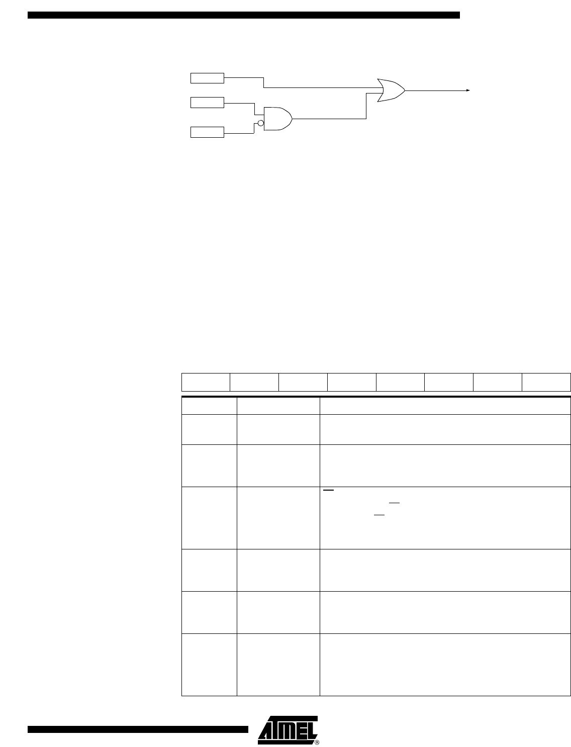
Figure 42. SPI Interrupt Requests Generation
Registers
There are three registers in the Module that provide control, status and data storage functions. These registers
are describes in the following paragraphs.
Serial Peripheral Control
Register (SPCON)
• The Serial Peripheral Control Register does the following:
• Selects one of the Master clock rates
• Configure the SPI Module as Master or Slave
• Selects serial clock polarity and phase
• Enables the SPI Module
• Frees the SS pin for a general-purpose
Table 79 describes this register and explains the use of each bit
Table 79. SPCON Register
SPCON - Serial Peripheral Control Register (0C3H)
SSDIS
MODF
CPU Interrupt Request
SPI Receiver/error
CPU Interrupt Request
SPI Transmitter
SPI
CPU Interrupt Request
SPIF
Table 1.
76543210
SPR2 SPEN SSDIS MSTR CPOL CPHA SPR1 SPR0
Bit Number Bit Mnemonic Description
7 SPR2
Serial Peripheral Rate 2
Bit with SPR1 and SPR0 define the clock rate.
6 SPEN
Serial Peripheral Enable
Cleared to disable the SPI interface.
Set to enable the SPI interface.
5 SSDIS
SS Disable
Cleared to enable SS in both Master and Slave modes.
Set to disable SS
in both Master and Slave modes. In Slave mode,
this bit has no effect if CPHA =’0’. When SSDIS is set, no MODF
interrupt request is generated
.
4MSTR
Serial Peripheral Master
Cleared to configure the SPI as a Slave.
Set to configure the SPI as a Master.
3CPOL
Clock Polarity
Cleared to have the SCK set to ’0’ in idle state.
Set to have the SCK set to ’1’ in idle low.
2CPHA
Clock Phase
Cleared to have the data sampled when the SCK leaves the idle
state (see CPOL).
Set to have the data sampled when the SCK returns to idle state (see
CPOL).