
Datasheet


Table Of Contents
- Features
- Description
- Block Diagram
- SFR Mapping
- Pin Configurations
- Oscillators
- Enhanced Features
- Dual Data Pointer Register DPTR
- Expanded RAM (XRAM)
- Reset
- Power Monitor
- Timer 2
- Programmable Counter Array PCA
- Serial I/O Port
- Interrupt System
- Power Management
- Keyboard Interface
- 2-wire Interface (TWI)
- Serial Port Interface (SPI)
- Hardware Watchdog Timer
- ONCE(TM) Mode (ON Chip Emulation)
- Power-off Flag
- EEPROM Data Memory
- Reduced EMI Mode
- Flash Memory
- Electrical Characteristics
- Absolute Maximum Ratings
- DC Parameters
- AC Parameters
- Explanation of the AC Symbols
- External Program Memory Characteristics
- External Program Memory Read Cycle
- External Data Memory Characteristics
- External Data Memory Write Cycle
- External Data Memory Read Cycle
- Serial Port Timing - Shift Register Mode
- Shift Register Timing Waveforms
- External Clock Drive Waveforms
- AC Testing Input/Output Waveforms
- Float Waveforms
- Clock Waveforms
- Ordering Information
- Packaging Information
- Table of Contents
102
AT89C51ID2
4289C–8051–11/05
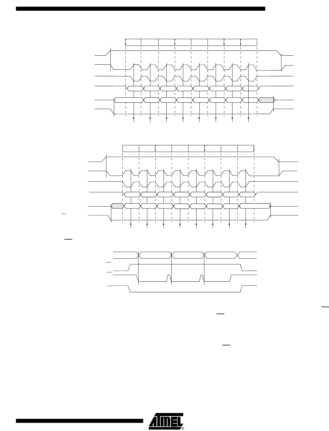
Figure 39. Data Transmission Format (CPHA = 0)
Figure 40. Data Transmission Format (CPHA = 1)
Figure 41. CPHA/SS
Timing
As shown in Figure 39, the first SCK edge is the MSB capture strobe. Therefore, the
Slave must begin driving its data before the first SCK edge, and a falling edge on the SS
pin is used to start the transmission. The SS pin must be toggled high and then low
between each Byte transmitted (Figure 41).
Figure 40 shows an SPI transmission in which CPHA is ’1’. In this case, the Master
begins driving its MOSI pin on the first SCK edge. Therefore, the Slave uses the first
SCK edge as a start transmission signal. The SS
pin can remain low between transmis-
sions (Figure 41). This format may be preffered in systems having only one Master and
only one Slave driving the MISO data line.
MSB bit6 bit5 bit4 bit3 bit2 bit1 LSB
bit6 bit5 bit4 bit3 bit2 bit1MSB
LSB
13245678
Capture Point
SS (to Slave)
MISO (from Slave)
MOSI (from Master)
SCK (CPOL = 1)
SCK (CPOL = 0)
SPEN (Internal)
SCK Cycle Number
MSB bit6 bit5 bit4 bit3 bit2 bit1 LSB
bit6 bit5 bit4 bit3 bit2 bit1
MSB LSB
13245678
Capture Point
SS
(to Slave)
MISO (from Slave)
MOSI (from Master)
SCK (CPOL = 1)
SCK (CPOL = 0)
SPEN (Internal)
SCK Cycle Number
Byte 1 Byte 2
Byte 3
MISO/MOSI
Master SS
Slave SS
(CPHA = 1)
Slave SS
(CPHA = 0)