
Datasheet
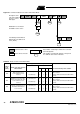
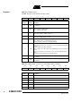
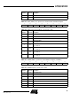
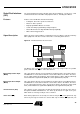
Table Of Contents
- Features
- Description
- Block Diagram
- SFR Mapping
- Pin Configurations
- Oscillators
- Enhanced Features
- Dual Data Pointer Register DPTR
- Expanded RAM (XRAM)
- Reset
- Power Monitor
- Timer 2
- Programmable Counter Array PCA
- Serial I/O Port
- Interrupt System
- Power Management
- Keyboard Interface
- 2-wire Interface (TWI)
- Serial Port Interface (SPI)
- Hardware Watchdog Timer
- ONCE(TM) Mode (ON Chip Emulation)
- Power-off Flag
- EEPROM Data Memory
- Reduced EMI Mode
- Flash Memory
- Electrical Characteristics
- Absolute Maximum Ratings
- DC Parameters
- AC Parameters
- Explanation of the AC Symbols
- External Program Memory Characteristics
- External Program Memory Read Cycle
- External Data Memory Characteristics
- External Data Memory Write Cycle
- External Data Memory Read Cycle
- Serial Port Timing - Shift Register Mode
- Shift Register Timing Waveforms
- External Clock Drive Waveforms
- AC Testing Input/Output Waveforms
- Float Waveforms
- Clock Waveforms
- Ordering Information
- Packaging Information
- Table of Contents
100
AT89C51ID2
4289C–8051–11/05
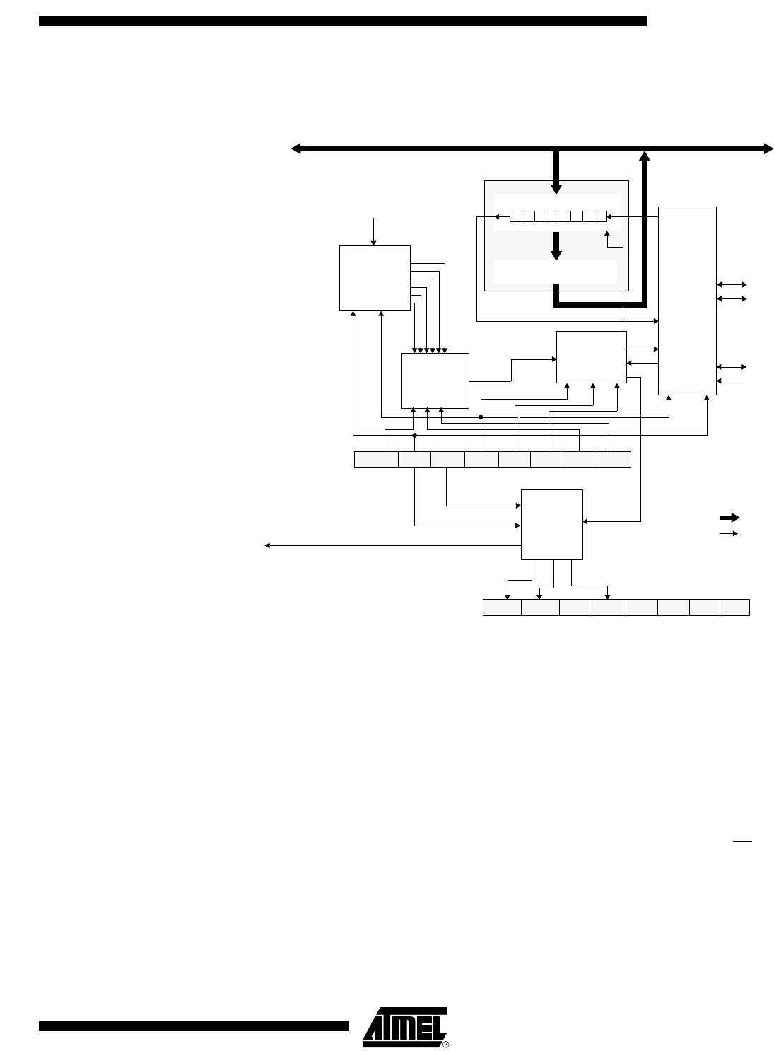
Functional Description Figure 37 shows a detailed structure of the SPI Module.
Figure 37. SPI Module Block Diagram
Operating Modes The Serial Peripheral Interface can be configured in one of the two modes: Master
mode or Slave mode. The configuration and initialization of the SPI Module is made
through one register:
• The Serial Peripheral Control register (SPCON)
Once the SPI is configured, the data exchange is made using:
• SPCON
• The Serial Peripheral STAtus register (SPSTA)
• The Serial Peripheral DATa register (SPDAT)
During an SPI transmission, data is simultaneously transmitted (shifted out serially) and
received (shifted in serially). A serial clock line (SCK) synchronizes shifting and sam-
pling on the two serial data lines (MOSI and MISO). A Slave Select line (SS
) allows
individual selection of a Slave SPI device; Slave devices that are not selected do not
interfere with SPI bus activities.
When the Master device transmits data to the Slave device via the MOSI line, the Slave
device responds by sending data to the Master device via the MISO line. This implies
full-duplex transmission with both data out and data in synchronized with the same clock
(Figure 38).
Shift Register
01
234567
Internal Bus
Pin
Control
Logic
MISO
MOSI
SCK
M
S
Clock
Logic
Clock
Divider
Clock
Select
/4
/64
/128
SPI Interrupt Request
8-bit bus
1-bit signal
SS
FCLK PERIPH
/32
/8
/16
Receive Data Register
SPDAT
SPI
Control
SPSTA
CPHA
SPR0
SPR1
CPOLMSTRSSDISSPEN
SPR2
SPCON
WCOL MODFSPIF
- ----