Features • 80C52 Compatible • • • • • • • • • • • • • • • • • • • • • • • • – 8051 Instruction Compatible – Six 8-bit I/O Ports (64 pins or 68 Pins Versions) – Four 8-bit I/O Ports (44 Pins Version) – Three 16-bit Timer/Counters – 256 bytes Scratch Pad RAM – 10 Interrupt Sources With 4 Priority Levels ISP (In-System Programming) Using Standard VCC Power Supply Integrated Power Monitor (POR/PFD) to Supervise Internal Power Supply Boot ROM Contains Low Level Flash Programming Routines and a Default Serial
The AT89C51ID2 retains all features of the Atmel 80C52 with 256 bytes of internal RAM, a 10-source 4-level interrupt controller and three timer/counters. In addition, the AT89C51ID2 has a Programmable Counter Array, an XRAM of 1792 bytes, a Hardware Watchdog Timer, SPI and Keyboard, a more versatile serial channel that facilitates multiprocessor communication (EUART) and a speed improvement mechanism (X2 mode).
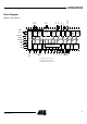
AT89C51ID2 Block Diagram (2) (2) (1) (1) (1) Keyboard T2 T2EX PCA ECI Vss VCC TxD RxD Figure 1.
AT89C51ID2 SFR Mapping The Special Function Registers (SFRs) of the AT89C51ID2 fall into the following categories: • C51 core registers: ACC, B, DPH, DPL, PSW, SP • I/O port registers: P0, P1, P2, P3, PI2 • Timer registers: T2CON, T2MOD, TCON, TH0, TH1, TH2, TMOD, TL0, TL1, TL2, RCAP2L, RCAP2H • Serial I/O port registers: SADDR, SADEN, SBUF, SCON • PCA (Programmable Counter Array) registers: CCON, CCAPMx, CL, CH, CCAPxH, CCAPxL (x: 0 to 4) • Power and clock control registers: PCON • Hardware W
Table 2. C51 Core SFRs Mnemonic Add Name ACC E0h Accumulator B F0h B Register PSW D0h Program Status Word SP 81h Stack Pointer DPL 82h Data Pointer Low byte DPH 83h Data Pointer High byte 7 6 5 4 3 2 1 0 CY AC F0 RS1 RS0 OV F1 P 7 6 5 4 3 2 1 0 SMOD1 SMOD0 - POF GF1 GF0 PD IDL XRS1 XRS0 EXTRA M AO Table 3.
AT89C51ID2 Table 5. Port SFRs Mnemonic Add Name P0 80h 8-bit Port 0 P1 90h 8-bit Port 1 P2 A0h 8-bit Port 2 P3 B0h 8-bit Port 3 P4 C0h 8-bit Port 4 P5 E8h 8-bit Port 5 P5 C7h 8-bit Port 5 (byte addressable) 7 6 5 4 3 2 1 0 - - - - 7 6 5 4 3 2 1 0 FPL3 FPL2 FPL1 FPL0 FPS FMOD1 FMOD0 FBUSY 7 6 5 4 3 2 1 0 Table 6. Flash and EEPROM Data Memory SFR Mnemonic FCON Add Name D1h Flash Control EECON EEPROM data Control Table 7.
Table 8.
AT89C51ID2 Table 11. Two-Wire Interface Controller SFRs Mnemonic Add Name 7 6 5 4 3 2 1 0 SSCON 93h Synchronous Serial control SSCR2 SSPE SSSTA SSSTO SSI SSAA SSCR1 SSCR0 SSCS 94h Synchronous Serial Status SSC4 SSC3 SSC2 SSC1 SSC0 0 0 0 SSDAT 95h Synchronous Serial Data SSD7 SSD6 SSD5 SSD4 SSD3 SSD2 SSD1 SSD0 SSADR 96h Synchronous Serial Address SSA7 SSA6 SSA5 SSA4 SSA3 SSA2 SSA1 SSGC 7 6 5 4 3 2 1 0 Table 12.
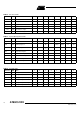
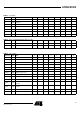
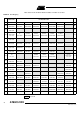
Table below shows all SFRs with their address and their reset value. Table 14.
AT89C51ID2 P0.2/AD2 P0.3/AD3 P0.1/AD1 P0.0/AD0 VCC XTALB2 P1.0/T2/XTALB1 P1.1/T2EX/SS P1.2/ECI P1.3/CEX0 P1.4/CEX1 Pin Configurations 6 5 4 3 2 1 44 43 42 41 40 P1.5/CEX2/MISO 39 38 P0.4/AD4 P1.6/CEX3/SCK 7 8 P1.7/CEx4/MOSI 9 37 P0.6/AD6 RST 10 36 P0.7/AD7 P3.0/RxD 35 34 EA PI2.1/SDA 11 12 P3.1/TxD 13 33 ALE/PROG P3.2/INT0 P3.3/INT1 14 15 32 31 PSEN P3.4/T0 P3.5/T1 16 30 P2.6/A14 17 29 P2.5/A13 AT89C51ID2 PLCC44 P0.5/AD5 PI2.0/SCL P2.7/A15 P0.3/AD3 P0.
Table 15. Pin Description Pin Number Type Mnemonic PLCC44 VQFP44 VSS 22 16 I Ground: 0V reference VCC 44 38 I Power Supply: This is the power supply voltage for normal, idle and power-down operation 43 - 36 37 - 30 P0.0 - P0.7 Name and Function I/O P1.0 - P1.7 2-9 40 - 44 1-3 I/O Port 0: Port 0 is an open-drain, bidirectional I/O port. Port 0 pins that have 1s written to them float and can be used as high impedance inputs.
AT89C51ID2 Table 15. Pin Description (Continued) Pin Number Type Mnemonic PLCC44 VQFP44 Name and Function I/O MOSI: SPI Master Output Slave Input line When SPI is in master mode, MOSI outputs data to the slave peripheral. When SPI is in slave mode, MOSI receives data from the master controller. XTALA1 21 15 I Crystal A 1: Input to the inverting oscillator amplifier and input to the internal clock generator circuits.
Table 15. Pin Description (Continued) Pin Number Type Mnemonic PLCC44 VQFP44 Name and Function SDA (PI2.1): 2-wire Serial Data 12 6 I/O SDA is the bidirectional 2-wire data line Reset: A high on this pin for two machine cycles while the oscillator is running, resets the device. An internal diffused resistor to VSS permits a power-on reset using only an external capacitor to VCC. This pin is an output when the hardware watchdog forces a system reset.
AT89C51ID2 Oscillators Overview Two oscillators are available (for AT8xC51IxD2 devices only, the others part number provide only the main high frequency oscillator): • OSCA used for high frequency: Up to 40 MHz • OSCB used for low frequency: 32.
Table 17.
AT89C51ID2 Table 19. PCON Register PCON - Power Control Register (87h) 7 6 5 4 3 2 1 0 SMOD1 SMOD0 - POF GF1 GF0 PD IDL Bit Number Bit Mnemonic Description 7 SMOD1 Serial port Mode bit 1 Set to select double baud rate in mode 1, 2 or 3. 6 SMOD0 Serial port Mode bit 0 Cleared to select SM0 bit in SCON register. Set to select FE bit in SCON register. 5 - Reserved The value read from this bit is indeterminate. Do not set this bit.
Functional Block Diagram Figure 2. Functional Oscillator Block Diagram Reload Reset PwdOscA CKRL FOSCA XtalA1 OscA 1 XtalA2 :2 0 OscAEn OSCCON 8-bit Prescaler-Divider 0 1 X2 1 CKCON0 CLK Peripheral Clock PERIPH 0 CLK CPU CKRL=0xFF? FOSCB CKS CPU clock Idle CKSEL PwdOscB XtalB1 XtalB2 :128 OscB Sub Clock OscBEn OSCCON Operating Modes Reset A hardware RESET puts the Clock generator in the following state: The selected oscillator depends on OSC bit in Hardware Security Byte (HSB).
AT89C51ID2 Idle Modes Power Down Modes • IDLE modes are achieved by using any instruction that writes into PCON.0 bit (IDL) • IDLE modes A and B depend on previous software sequence, prior to writing into PCON.0 bit: • IDLE MODE A: OscA is running (OscAEn = 1) and selected (CKS = 1) • IDLE MODE B: OscB is running (OscBEn = 1) and selected (CKS = 0) • The unused oscillator OscA or OscB can be stopped by software by clearing OscAEn or OscBEn respectively.
Table 20. Overview (Continued) PCON.1 PCON.0 OscBEn OscAEn CKS Selected Mode Comment 0 1 1 X 0 IDLE MODE B The CPU is off, OscB supplies the peripherals, OscA can be disabled (OscAEn = 0) 1 X X 1 X POWER DOWN MODE The CPU and peripherals are off, OscA and OscB are stopped Design Considerations Oscillators Control Prescaler Divider • PwdOscA and PwdOscB signals are generated in the Clock generator and used to control the hard blocks of oscillators A and B.
AT89C51ID2 – FCLK CPU and FCLK PERIPH, for CKRL≠0xFF In X2 Mode: F OSCA F CPU = F CLKPERIPH = --------------------------------------------- 2 × ( 255 – CKRL ) In X1 Mode: F OSCA F CPU = F CLKPERIPH = --------------------------------------------- 4 × ( 255 – CKRL ) Timer 0: Clock Inputs Figure 1.
AT89C51ID2 Enhanced Features X2 Feature In comparison to the original 80C52, the AT89C51ID2 implements some new features, which are: • X2 option • Dual Data Pointer • Extended RAM • Programmable Counter Array (PCA) • Hardware Watchdog • SPI interface • 4-level interrupt priority system • power-off flag • ONCE mode • ALE disabling • Enhanced features on the UART and the timer 2 The AT89C51ID2 core needs only 6 clock periods per machine cycle.
Figure 4. Mode Switching Waveforms XTAL1 XTAL1:2 X2 bit FOSC CPU clock STD Mode X2 Mode STD Mode The X2 bit in the CKCON0 register (see Table 21) allows a switch from 12 clock periods per instruction to 6 clock periods and vice versa. At reset, the speed is set according to X2 bit of Hardware Security Byte (HSB). By default, Standard mode is active. Setting the X2 bit activates the X2 feature (X2 mode). The T0X2, T1X2, T2X2, UartX2, PcaX2, and WdX2 bits in the CKCON0 register (See Table 21.
AT89C51ID2 Table 21. CKCON0 Register CKCON0 - Clock Control Register (8Fh) 7 6 5 4 3 2 1 0 TWIX2 WDX2 PCAX2 SIX2 T2X2 T1X2 T0X2 X2 Bit Number 7 Bit Mnemonic Description TWIX2 2-wire clock (This control bit is validated when the CPU clock X2 is set; when X2 is low, this bit has no effect) Cleared to select 6 clock periods per peripheral clock cycle. Set to select 12 clock periods per peripheral clock cycle.
Table 22. CKCON1 Register CKCON1 - Clock Control Register (AFh) 7 6 5 4 3 2 1 0 - - - - - - - SPIX2 Bit Number Bit Mnemonic Description 7 - Reserved 6 - Reserved 5 - Reserved 4 - Reserved 3 - Reserved 2 - Reserved 1 - Reserved 0 SPIX2 SPI (This control bit is validated when the CPU clock X2 is set; when X2 is low, this bit has no effect). Clear to select 6 clock periods per peripheral clock cycle. Set to select 12 clock periods per peripheral clock cycle.
AT89C51ID2 Dual Data Pointer Register DPTR The additional data pointer can be used to speed up code execution and reduce code size. The dual DPTR structure is a way by which the chip will specify the address of an external data memory location. There are two 16-bit DPTR registers that address the external memory, and a single bit called DPS = AUXR1.0 (see Table 23) that allows the program code to switch between them (Refer to Figure 5). Figure 5.
Table 23. AUXR1 register AUXR1- Auxiliary Register 1(0A2h) 7 6 5 4 3 2 1 0 - - ENBOOT - GF3 0 - DPS Bit Bit Number Mnemonic Description 7 - Reserved The value read from this bit is indeterminate. Do not set this bit. 6 - Reserved The value read from this bit is indeterminate. Do not set this bit. 5 ENBOOT Enable Boot Flash Cleared to disable boot ROM. Set to map the boot ROM between F800h - 0FFFFh. Reserved The value read from this bit is indeterminate. Do not set this bit.
AT89C51ID2 INC is a short (2 bytes) and fast (12 clocks) way to manipulate the DPS bit in the AUXR1 SFR. However, note that the INC instruction does not directly force the DPS bit to a particular state, but simply toggles it. In simple routines, such as the block move example, only the fact that DPS is toggled in the proper sequence matters, not its actual value. In other words, the block move routine works the same whether DPS is '0' or '1' on entry.
AT89C51ID2 Expanded RAM (XRAM) The AT89C51ID2 provides additional Bytes of random access memory (RAM) space for increased data parameter handling and high level language usage. AT89C51ID2 devices have expanded RAM in external data space configurable up to 1792bytes (see Table 24.). The AT89C51ID2 has internal data memory that is mapped into four separate segments. The four segments are: 1. The Lower 128 bytes of RAM (addresses 00h to 7Fh) are directly and indirectly addressable. 2.
useful if external peripherals are mapped at addresses already used by the internal XRAM. • With EXTRAM = 0, the XRAM is indirectly addressed, using the MOVX instruction in combination with any of the registers R0, R1 of the selected bank or DPTR. An access to XRAM will not affect ports P0, P2, P3.6 (WR) and P3.7 (RD). For example, with EXTRAM = 0, MOVX @R0, # data where R0 contains 0A0H, accesses the XRAM at address 0A0H rather than external memory.
AT89C51ID2 Registers Table 24. AUXR Register AUXR - Auxiliary Register (8Eh) 7 6 5 4 3 2 1 0 - - M0 XRS2 XRS1 XRS0 EXTRAM AO Bit Number Bit Mnemonic Description 7 - 6 - Reserved The value read from this bit is indeterminate. Do not set this bit. Reserved The value read from this bit is indeterminate. Do not set this bit. Pulse length 5 M0 Cleared to stretch MOVX control: the RD/ and the WR/ pulse length is 6 clock periods (default).
AT89C51ID2 Reset Introduction The reset sources are : Power Management, Hardware Watchdog, PCA Watchdog and Reset input. Figure 7. Reset schematic Power Monitor Hardware Watchdog Internal Reset PCA Watchdog RST Reset Input The Reset input can be used to force a reset pulse longer than the internal reset controlled by the Power Monitor. RST input has a pull-down resistor allowing power-on reset by simply connecting an external capacitor to VCC as shown in Figure 8.
Reset Output As detailed in Section “Hardware Watchdog Timer”, page 107, the WDT generates a 96clock period pulse on the RST pin. In order to properly propagate this pulse to the rest of the application in case of external capacitor or power-supply supervisor circuit, a 1 kΩ resistor must be added as shown Figure 9. Figure 9.
AT89C51ID2 Power Monitor The POR/PFD function monitors the internal power-supply of the CPU core memories and the peripherals, and if needed, suspends their activity when the internal power supply falls below a safety threshold. This is achieved by applying an internal reset to them. By generating the Reset the Power Monitor insures a correct start up when AT89C51ID2 is powered up.
The Power fail detect monitor the supply generated by the voltage regulator and generate a reset if this supply falls below a safety threshold as illustrated in the Figure 11 below. Figure 11. Power Fail Detect Vcc t Reset Vcc When the power is applied, the Power Monitor immediately asserts a reset. Once the internal supply after the voltage regulator reach a safety level, the power monitor then looks at the XTAL clock input.
AT89C51ID2 Timer 2 The Timer 2 in the AT89C51ID2 is the standard C52 Timer 2. It is a 16-bit timer/counter: the count is maintained by two eight-bit timer registers, TH2 and TL2 are cascaded. It is controlled by T2CON (Table 25) and T2MOD (Table 26) registers. Timer 2 operation is similar to Timer 0 and Timer 1.C/T2 selects FOSC/12 (timer operation) or external pin T2 (counter operation) as the timer clock input. Setting TR2 allows TL2 to increment by the selected input.
Figure 12. Auto-Reload Mode Up/Down Counter (DCEN = 1) FCLK PERIPH :6 0 1 T2 C/T2 TR2 T2CON T2CON T2EX: (DOWN COUNTING RELOAD VALUE) if DCEN=1, 1=UP FFh FFh if DCEN=1, 0=DOWN (8-bit) (8-bit) if DCEN = 0, up counting TOGGLE T2CON EXF2 TL2 TH2 (8-bit) (8-bit) TIMER 2 INTERRUPT TF2 T2CON RCAP2L (8-bit) RCAP2H (8-bit) (UP COUNTING RELOAD VALUE) Programmable ClockOutput In the clock-out mode, Timer 2 operates as a 50%-duty-cycle, programmable clock generator (See Figure 13).
AT89C51ID2 Figure 13.
Registers Table 25. T2CON Register T2CON - Timer 2 Control Register (C8h) 7 6 5 4 3 2 1 0 TF2 EXF2 RCLK TCLK EXEN2 TR2 C/T2# CP/RL2# Bit Number 7 Bit Mnemonic Description TF2 Timer 2 overflow Flag Must be cleared by software. Set by hardware on Timer 2 overflow, if RCLK = 0 and TCLK = 0. 6 EXF2 Timer 2 External Flag Set when a capture or a reload is caused by a negative transition on T2EX pin if EXEN2=1.
AT89C51ID2 Table 26. T2MOD Register T2MOD - Timer 2 Mode Control Register (C9h) 7 6 5 4 3 2 1 0 - - - - - - T2OE DCEN Bit Number Bit Mnemonic Description 7 - Reserved The value read from this bit is indeterminate. Do not set this bit. 6 - Reserved The value read from this bit is indeterminate. Do not set this bit. 5 - Reserved The value read from this bit is indeterminate. Do not set this bit. 4 - Reserved The value read from this bit is indeterminate. Do not set this bit.
AT89C51ID2 Programmable Counter Array PCA The PCA provides more timing capabilities with less CPU intervention than the standard timer/counters. Its advantages include reduced software overhead and improved accuracy. The PCA consists of a dedicated timer/counter which serves as the time base for an array of five compare/capture modules.
Figure 14. PCA Timer/Counter To PCA modules Fclk periph /6 overflow Fclk periph / 2 CH T0 OVF It CL 16 bit up counter P1.
AT89C51ID2 Table 27. CMOD Register CMOD - PCA Counter Mode Register (D9h) 7 6 5 4 3 2 1 0 CIDL WDTE - - - CPS1 CPS0 ECF Bit Number Bit Mnemonic Description Counter Idle Control 7 CIDL Cleared to program the PCA Counter to continue functioning during idle Mode. Set to program PCA to be gated off during idle. Watchdog Timer Enable 6 WDTE Cleared to disable Watchdog Timer function on PCA Module 4. Set to enable Watchdog Timer function on PCA Module 4.
• Bits 0 through 4 are the flags for the modules (bit 0 for module 0, bit 1 for module 1, etc.) and are set by hardware when either a match or a capture occurs. These flags also can only be cleared by software. Table 28. CCON Register CCON - PCA Counter Control Register (D8h) 7 6 5 4 3 2 1 0 CF CR - CCF4 CCF3 CCF2 CCF1 CCF0 Bit Number Bit Mnemonic Description PCA Counter Overflow flag 7 CF Set by hardware when the counter rolls over. CF flags an interrupt if bit ECF in CMOD is set.
AT89C51ID2 Figure 15. PCA Interrupt System CF CR CCF4 CCF3 CCF2 CCF1 CCF0 CCON 0xD8 PCA Timer/Counter Module 0 Module 1 To Interrupt priority decoder Module 2 Module 3 Module 4 CMOD.0 ECF ECCFn CCAPMn.0 IEN0.6 EC IEN0.7 EA PCA Modules: each one of the five compare/capture modules has six possible functions.
Table 29 shows the CCAPMn settings for the various PCA functions. Table 29.
AT89C51ID2 Table 30. PCA Module Modes (CCAPMn Registers) ECOMn CAPPn CAPNn MATn TOGn PWMm ECCFn Module Function 0 0 0 0 0 0 0 No Operation X 1 0 0 0 0 X 16-bit capture by a positive-edge trigger on CEXn X 0 1 0 0 0 X 16-bit capture by a negative trigger on CEXn X 1 1 0 0 0 X 16-bit capture by a transition on CEXn 1 0 0 1 0 0 X 16-bit Software Timer / Compare mode.
Table 32.
AT89C51ID2 PCA Capture Mode To use one of the PCA modules in the capture mode either one or both of the CCAPM bits CAPN and CAPP for that module must be set. The external CEX input for the module (on port 1) is sampled for a transition. When a valid transition occurs the PCA hardware loads the value of the PCA counter registers (CH and CL) into the module's capture registers (CCAPnL and CCAPnH).
Figure 17. PCA Compare Mode and PCA Watchdog Timer CCON CF Write to CCAPnL CR CCF4 CCF3 CCF2 CCF1 CCF0 0xD8 Reset PCA IT Write t o CCAPnH 1 CCAPnH 0 CCAPnL Enable Match 16 bit comparator CH RESET * CL PCA counter/timer ECOMn CAPPn CAPNn MATn TOGn PWMn ECCFn CIDL WDTE CPS1 CPS0 ECF CCAPMn, n = 0 to 4 0xDA to 0xDE CMOD 0xD9 Before enabling ECOM bit, CCAPnL and CCAPnH should be set with a non zero value, otherwise an unwanted match could happen. Writing to CCAPnH will set the ECOM bit.
AT89C51ID2 Figure 18. PCA High Speed Output Mode CCON CF CR CCF4 CCF3 CCF2 CCF1 CCF0 0xD8 Write to CCA PnL Reset PCA IT Write to CCAPnH 1 CCAPnH 0 CCAPnL Enable 16 bit comparator CH Match CL CEXn PCA counter/timer ECOMn CAPPn CAPNn MATn TOGn PWMn ECCFn CCAPMn, n = 0 to 4 0xDA to 0xDE Before enabling ECOM bit, CCAPnL and CCAPnH should be set with a non zero value, otherwise an unwanted match could happen.
Figure 19. PCA PWM Mode CCAPnH Overflow CCAPnL “0” CEXn Enable 8 bit comparator “1” CL PCA counter/timer ECOMn CAPPn CAPNn MATn TOGn PWMn ECCFn CCAPMn, n= 0 to 4 0xDA to 0xDE PCA Watchdog Timer An on-board watchdog timer is available with the PCA to improve the reliability of the system without increasing chip count. Watchdog timers are useful for systems that are susceptible to noise, power glitches, or electrostatic discharge. Module 4 is the only PCA module that can be programmed as a watchdog.
AT89C51ID2 Serial I/O Port The serial I/O port in the AT89C51ID2 is compatible with the serial I/O port in the 80C52. It provides both synchronous and asynchronous communication modes. It operates as a Universal Asynchronous Receiver and Transmitter (UART) in three full-duplex modes (Modes 1, 2 and 3).
Figure 22. UART Timings in Modes 2 and 3 RXD D0 Start bit D1 D2 D3 D4 Data byte D5 D6 D7 D8 Ninth Stop bit bit RI SMOD0=0 RI SMOD0=1 FE SMOD0=1 Automatic Address Recognition The automatic address recognition feature is enabled when the multiprocessor communication feature is enabled (SM2 bit in SCON register is set).
AT89C51ID2 The SADEN byte is selected so that each slave may be addressed separately. For slave A, bit 0 (the LSB) is a don’t-care bit; for slaves B and C, bit 0 is a 1.To communicate with slave A only, the master must send an address where bit 0 is clear (e. g. 1111 0000b). For slave A, bit 1 is a 1; for slaves B and C, bit 1 is a don’t care bit. To communicate with slaves B and C, but not slave A, the master must send an address with bits 0 and 1 both set (e. g. 1111 0011b).
Registers Table 35. SADEN Register SADEN - Slave Address Mask Register (B9h) 7 6 5 4 3 2 1 0 3 2 1 0 Reset Value = 0000 0000b Not bit addressable Table 36. SADDR Register SADDR - Slave Address Register (A9h) 7 6 5 4 Reset Value = 0000 0000b Not bit addressable Baud Rate Selection for UART for Mode 1 and 3 The Baud Rate Generator for transmit and receive clocks can be selected separately via the T2CON and BDRCON registers. Figure 23.
AT89C51ID2 Table 37.
Table 38. SCON Register SCON - Serial Control Register (98h) 7 6 5 4 3 2 1 0 FE/SM0 SM1 SM2 REN TB8 RB8 TI RI Bit Bit Number Mnemonic Description Framing Error bit (SMOD0=1) FE Clear to reset the error state, not cleared by a valid stop bit. Set by hardware when an invalid stop bit is detected. SMOD0 must be set to enable access to the FE bit. 7 SM0 Serial port Mode bit 0 Refer to SM1 for serial port mode selection. SMOD0 must be cleared to enable access to the SM0 bit.
AT89C51ID2 Table 39. Example of Computed Value When X2=1, SMOD1=1, SPD=1 Baud Rates FOSC = 16. 384 MHz FOSC = 24MHz BRL Error (%) BRL Error (%) 115200 247 1.23 243 0.16 57600 238 1.23 230 0.16 38400 229 1.23 217 0.16 28800 220 1.23 204 0.16 19200 203 0.63 178 0.16 9600 149 0.31 100 0.16 4800 43 1.23 - - Table 40. Example of Computed Value When X2=0, SMOD1=0, SPD=0 Baud Rates FOSC = 16. 384 MHz FOSC = 24MHz BRL Error (%) BRL Error (%) 4800 247 1.23 243 0.
Table 43. SBUF Register SBUF - Serial Buffer Register for UART (99h) 7 6 5 4 3 2 1 0 Reset Value = XXXX XXXXb Table 44.
AT89C51ID2 Table 45. T2CON Register T2CON - Timer 2 Control Register (C8h) 7 6 5 4 3 2 1 0 TF2 EXF2 RCLK TCLK EXEN2 TR2 C/T2# CP/RL2# Bit Bit Number Mnemonic 7 TF2 Description Timer 2 overflow Flag Must be cleared by software. Set by hardware on timer 2 overflow, if RCLK = 0 and TCLK = 0. 6 EXF2 Timer 2 External Flag Set when a capture or a reload is caused by a negative transition on T2EX pin if EXEN2=1.
Table 46. PCON Register PCON - Power Control Register (87h) 7 6 5 4 3 2 1 0 SMOD1 SMOD0 - POF GF1 GF0 PD IDL Bit Bit Number Mnemonic 7 SMOD1 6 SMOD0 5 - 4 POF Power-Off Flag Cleared to recognize next reset type. Set by hardware when VCC rises from 0 to its nominal voltage. Can also be set by software. 3 GF1 General purpose Flag Cleared by user for general purpose usage. Set by user for general purpose usage.
AT89C51ID2 Table 47. BDRCON Register BDRCON - Baud Rate Control Register (9Bh) 7 6 5 4 3 2 1 0 - - - BRR TBCK RBCK SPD SRC Bit Number Bit Mnemonic 7 - Reserved The value read from this bit is indeterminate. Do not set this bit 6 - Reserved The value read from this bit is indeterminate. Do not set this bit 5 - Reserved The value read from this bit is indeterminate. Do not set this bit. 4 BRR Baud Rate Run Control bit Cleared to stop the internal Baud Rate Generator.
AT89C51ID2 Interrupt System The AT89C51ID2 has a total of 10 interrupt vectors: two external interrupts (INT0 and INT1), three timer interrupts (timers 0, 1 and 2), the serial port interrupt, SPI interrupt, Keyboard interrupt and the PCA global interrupt. These interrupts are shown in Figure 25. Figure 25.
Registers The PCA interrupt vector is located at address 0033H, the SPI interrupt vector is located at address 0043H and Keyboard interrupt vector is located at address 004BH. All other vectors addresses are the same as standard C52 devices. Table 48. Priority Level Bit Values IPH. x IPL. x Interrupt Level Priority 0 0 0 (Lowest) 0 1 1 1 0 2 1 1 3 (Highest) A low-priority interrupt can be interrupted by a high priority interrupt, but not by another low-priority interrupt.
AT89C51ID2 Table 49. IENO Register IEN0 - Interrupt Enable Register (A8h) 7 6 5 4 3 2 1 0 EA EC ET2 ES ET1 EX1 ET0 EX0 Bit Number Bit Mnemonic Description 7 EA 6 EC Enable All interrupt bit Cleared to disable all interrupts. Set to enable all interrupts. PCA interrupt enable bit Cleared to disable. Set to enable. 5 ET2 Timer 2 overflow interrupt Enable bit Cleared to disable timer 2 overflow interrupt. Set to enable timer 2 overflow interrupt.
Table 50. IPL0 Register IPL0 - Interrupt Priority Register (B8h) 7 6 5 4 3 2 1 0 - PPCL PT2L PSL PT1L PX1L PT0L PX0L Bit Number Bit Mnemonic Description Reserved The value read from this bit is indeterminate. Do not set this bit. 7 - 6 PPCL PCA interrupt Priority bit Refer to PPCH for priority level. 5 PT2L Timer 2 overflow interrupt Priority bit Refer to PT2H for priority level. 4 PSL Serial port Priority bit Refer to PSH for priority level.
AT89C51ID2 Table 51. IPH0 Register IPH0 - Interrupt Priority High Register (B7h) 7 6 5 4 3 2 1 0 - PPCH PT2H PSH PT1H PX1H PT0H PX0H Bit Number 7 6 5 4 3 2 1 0 Bit Mnemonic Description - Reserved The value read from this bit is indeterminate. Do not set this bit. PPCH PCA interrupt Priority high bit.
Table 52. IEN1 Register IEN1 - Interrupt Enable Register (B1h) 7 6 5 4 3 2 1 0 - - - - - ESPI ETWI EKBD Bit Number Bit Mnemonic Description 7 - Reserved 6 - Reserved 5 - Reserved 4 - Reserved 3 - Reserved 2 ESPI SPI interrupt Enable bit Cleared to disable SPI interrupt. Set to enable SPI interrupt. TWI interrupt Enable bit 1 ETWI Cleared to disable TWI interrupt. Set to enable TWI interrupt. 0 EKBD Keyboard interrupt Enable bit Cleared to disable keyboard interrupt.
AT89C51ID2 Table 53. IPL1 Register IPL1 - Interrupt Priority Register (B2h) Table 54. 7 6 5 4 3 2 1 0 - - - - - SPIL TWIL KBDL Bit Number Bit Mnemonic Description 7 - Reserved The value read from this bit is indeterminate. Do not set this bit. 6 - Reserved The value read from this bit is indeterminate. Do not set this bit. 5 - Reserved The value read from this bit is indeterminate. Do not set this bit. 4 - Reserved The value read from this bit is indeterminate.
Table 55. IPH1 Register IPH1 - Interrupt Priority High Register (B3h) 7 6 5 4 3 2 1 0 - - - - - SPIH TWIH KBDH Bit Number Bit Mnemonic Description 7 - Reserved The value read from this bit is indeterminate. Do not set this bit. 6 - Reserved The value read from this bit is indeterminate. Do not set this bit. 5 - Reserved The value read from this bit is indeterminate. Do not set this bit. 4 - Reserved The value read from this bit is indeterminate. Do not set this bit.
AT89C51ID2 Interrupt Sources and Vector Addresses Table 56.
AT89C51ID2 Power Management Introduction Two power reduction modes are implemented in the AT89C51ID2. The Idle mode and the Power-Down mode. These modes are detailed in the following sections. In addition to these power reduction modes, the clocks of the core and peripherals can be dynamically divided by 2 using the X2 mode detailed in Section “Enhanced Features”, page 21. Idle Mode Idle mode is a power reduction mode that reduces the power consumption. In this mode, program execution halts.
and RAM contents are preserved. The status of the Port pins during Power-Down mode is detailed in Table 57. Note: Entering Power-Down Mode VCC may be reduced to as low as VRET during Power-Down mode to further reduce power dissipation. Take care, however, that VDD is not reduced until Power-Down mode is invoked. To enter Power-Down mode, set PD bit in PCON register. The AT89C51ID2 enters the Power-Down mode upon execution of the instruction that sets PD bit.
AT89C51ID2 pins, the instruction immediately following the instruction that activated the Power-Down mode should not write to a Port pin or to the external RAM. Note: Exit from power-down by reset redefines all the SFRs, but does not affect the internal RAM content. Table 57.
Registers Table 58. PCON Register PCON (S87:h) Power configuration Register 7 6 5 4 3 2 1 0 - - - POF GF1 GF0 PD IDL Bit Number 7-5 Bit Mnemonic Description - Reserved The value read from these bits is indeterminate. Do not set these bits. 4 POF Power-Off Flag Cleared to recognize next reset type. Set by hardware when VCC rises from 0 to its nominal voltage. Can also be set by software.
AT89C51ID2 Keyboard Interface The AT89C51ID2 implements a keyboard interface allowing the connection of a 8 x n matrix keyboard. It is based on 8 inputs with programmable interrupt capability on both high or low level. These inputs are available as alternate function of P1 and allow to exit from idle and power down modes.
Registers Table 59. KBF Register KBF-Keyboard Flag Register (9Eh) 7 6 5 4 3 2 1 0 KBF7 KBF6 KBF5 KBF4 KBF3 KBF2 KBF1 KBF0 Bit Number 7 6 5 4 3 2 1 0 Bit Mnemonic Description KBF7 Keyboard line 7 flag Set by hardware when the Port line 7 detects a programmed level. It generates a Keyboard interrupt request if the KBKBIE. 7 bit in KBIE register is set. Must be cleared by software. KBF6 Keyboard line 6 flag Set by hardware when the Port line 6 detects a programmed level.
AT89C51ID2 Table 60. KBE Register KBE-Keyboard Input Enable Register (9Dh) 7 6 5 4 3 2 1 0 KBE7 KBE6 KBE5 KBE4 KBE3 KBE2 KBE1 KBE0 Bit Number Bit Mnemonic Description 7 KBE7 Keyboard line 7 Enable bit Cleared to enable standard I/O pin. Set to enable KBF. 7 bit in KBF register to generate an interrupt request. 6 KBE6 Keyboard line 6 Enable bit Cleared to enable standard I/O pin. Set to enable KBF. 6 bit in KBF register to generate an interrupt request.
Table 61. KBLS Register KBLS-Keyboard Level Selector Register (9Ch) 7 6 5 4 3 2 1 0 KBLS7 KBLS6 KBLS5 KBLS4 KBLS3 KBLS2 KBLS1 KBLS0 Bit Number Bit Mnemonic Description 7 KBLS7 Keyboard line 7 Level Selection bit Cleared to enable a low level detection on Port line 7. Set to enable a high level detection on Port line 7. 6 KBLS6 Keyboard line 6 Level Selection bit Cleared to enable a low level detection on Port line 6. Set to enable a high level detection on Port line 6.
AT89C51ID2 2-wire Interface (TWI) This section describes the 2-wire interface. The 2-wire bus is a bi-directional 2-wire serial communication standard. It is designed primarily for simple but efficient integrated circuit (IC) control. The system is comprised of two lines, SCL (Serial Clock) and SDA (Serial Data) that carry information between the ICs connected to them. The serial data transfer is limited to 400 Kbit/s in standard mode. Various communication configuration can be designed using this bus.
Figure 30. Block Diagram 8 Address Register SSADR Comparator Input Filter SDA PI2.1 Output Stage SSDAT ACK Shift Register Arbitration & Sink Logic Input Filter Timing & Control logic SCL PI2.
AT89C51ID2 Description The CPU interfaces to the 2-wire logic via the following four 8-bit special function registers: the Synchronous Serial Control register (SSCON; Table 71), the Synchronous Serial Data register (SSDAT; Table 72), the Synchronous Serial Control and Status register (SSCS; Table 73) and the Synchronous Serial Address register (SSADR Table 76).
W: Write bit (low level at SDA) A: Acknowledge bit (low level at SDA) A: Not acknowledge bit (high level at SDA) Data: 8-bit data byte P : STOP condition In Figure 32 to Figure 35, circles are used to indicate when the serial interrupt flag is set. The numbers in the circles show the status code held in SSCS. At these points, a service routine must be executed to continue or complete the serial transfer.
AT89C51ID2 When the slave address and the direction bit have been transmitted and an acknowledgement bit has been received, the serial interrupt flag is set again and a number of status code in SSCS are possible. There are 40h, 48h or 38h for the master mode and also 68h, 78h or B0h if the slave mode was enabled (AA=logic 1). The appropriate action to be taken for each of these status code is detailed in Table . This scheme is repeated until a STOP condition is transmitted.
its own slave address followed by the data direction bit which must be at logic 1 (R) for TWI to operate in the slave transmitter mode. After its own slave address and the R bit have been received, the serial interrupt flag is set and a valid status code can be read from SSCS. This status code is used to vector to an interrupt service routine. The appropriate action to be taken for each of these status code is detailed in Table .
AT89C51ID2 Figure 32.
Table 66. Status in Master Transmitter Mode Application software response Status Code SSSTA To SSCON To/From SSDAT SSSTA SSSTO SSI SSAA Next Action Taken by Two-wire Hardware 08h A START condition has Write SLA+W been transmitted X 0 0 X Write SLA+W X 0 0 X 10h A repeated START condition has been transmitted Write SLA+R X 0 0 X Write data byte 0 0 0 X No SSDAT action 1 0 0 X No SSDAT action 0 1 0 X STOP condition will be transmitted and SSSTO flag will be reset.
AT89C51ID2 Figure 33.
Table 67. Status in Master Receiver Mode Application software response Status Code SSSTA To SSCON To/From SSDAT SSSTA SSSTO SSI SSAA Next Action Taken by Two-wire Hardware 08h A START condition has Write SLA+R been transmitted X 0 0 X Write SLA+R X 0 0 X 10h A repeated START condition has been transmitted Write SLA+W X 0 0 X SLA+W will be transmitted. Logic will switch to master transmitter mode.
AT89C51ID2 Figure 34. Format and State in the Slave Receiver Mode Reception of the own slave address and one or more data bytes. All are acknowledged. S SLA W Data A 60h A Data 80h Last data byte received is not acknowledged. A P or S 80h A0h A P or S 88h Arbitration lost as master and addressed as slave A 68h Reception of the general call address and one or more data bytes. General Call Data A 70h Last data byte received is not acknowledged.
Table 68.
AT89C51ID2 Table 68.
Figure 35. Format and State in the Slave Transmitter Mode Reception of the S own slave address and one or more data bytes SLA A R Data A A8h Arbitration lost as master and addressed as slave B8h Data A P or S C0h A B0h Last data byte transmitted.
AT89C51ID2 Table 69.
Registers Table 71. SSCON Register SSCON - Synchronous Serial Control register (93h) 7 6 5 4 3 2 1 0 CR2 SSIE STA STO SI AA CR1 CR0 Bit Number Bit Mnemonic Description 7 CR2 Control Rate bit 2 See Table 65. 6 SSIE Synchronous Serial Interface Enable bit Clear to disable the TWI module. Set to enable the TWI module. 5 STA Start flag Set to send a START condition on the bus. 4 ST0 Stop flag Set to send a STOP condition on the bus.
AT89C51ID2 Bit Number Bit Mnemonic Description 1 SD1 Address bit 1 or Data bit 1. 0 SD0 Address bit 0 (R/W) or Data bit 0. Table 73. SSCS (094h) read - Synchronous Serial Control and Status Register 7 6 5 4 3 2 1 0 SC4 SC3 SC2 SC1 SC0 0 0 0 Table 74. SSCS Register: Read Mode - Reset Value = F8h Bit Number Bit Mnemonic Description 0 0 Always zero 1 0 Always zero 2 0 Always zero 3 SC0 4 SC1 5 SC2 Status Code bit 2 See to Table 70.
Bit Number Bit Mnemonic Description General Call bit 0 GC Clear to disable the general call address recognition. Set to enable the general call address recognition.
AT89C51ID2 Serial Port Interface (SPI) The Serial Peripheral Interface Module (SPI) allows full-duplex, synchronous, serial communication between the MCU and peripheral devices, including other MCUs.
drive the network. The Master may select each Slave device by software through port pins (Figure 37). To prevent bus conflicts on the MISO line, only one slave should be selected at a time by the Master for a transmission. In a Master configuration, the SS line can be used in conjunction with the MODF flag in the SPI Status register (SPSTA) to prevent multiple masters from driving MOSI and SCK (see Error conditions). A high level on the SS pin puts the MISO line of a Slave SPI in a high-impedance state.
AT89C51ID2 Functional Description Figure 37 shows a detailed structure of the SPI Module. Figure 37.
Figure 38. Full-Duplex Master-Slave Interconnection 8-bit Shift register SPI Clock Generator MISO MISO MOSI MOSI SCK SS Master MCU 8-bit Shift register SCK VDD SS VSS Slave MCU Master Mode The SPI operates in Master mode when the Master bit, MSTR (1), in the SPCON register is set. Only one Master SPI device can initiate transmissions. Software begins the transmission from a Master SPI Module by writing to the Serial Peripheral Data Register (SPDAT).
AT89C51ID2 Figure 39. Data Transmission Format (CPHA = 0) SCK Cycle Number 1 2 3 4 5 6 7 8 MSB bit6 bit5 bit4 bit3 bit2 bit1 LSB bit6 bit5 bit4 bit3 bit2 bit1 LSB SPEN (Internal) SCK (CPOL = 0) SCK (CPOL = 1) MOSI (from Master) MISO (from Slave) MSB SS (to Slave) Capture Point Figure 40.
Error Conditions The following flags in the SPSTA signal SPI error conditions: Mode Fault (MODF) Mode Fault error in Master mode SPI indicates that the level on the Slave Select (SS) pin is inconsistent with the actual mode of the device. MODF is set to warn that there may be a multi-master conflict for system control. In this case, the SPI system is affected in the following ways: • An SPI receiver/error CPU interrupt request is generated • The SPEN bit in SPCON is cleared.
AT89C51ID2 Figure 42. SPI Interrupt Requests Generation SPIF SPI Transmitter CPU Interrupt Request SPI CPU Interrupt Request MODF SPI Receiver/error CPU Interrupt Request SSDIS Registers There are three registers in the Module that provide control, status and data storage functions. These registers are describes in the following paragraphs.
Bit Number Bit Mnemonic SPR1 1 0 SPR0 Description SPR2 SPR1 0 0 SPR0 Serial Peripheral Rate 0 FCLK PERIPH /2 0 0 1 FCLK PERIPH /4 0 1 0 FCLK PERIPH /8 0 1 1 FCLK PERIPH /16 1 0 0 FCLK PERIPH /32 1 0 1 FCLK PERIPH /64 1 1 0 FCLK PERIPH /128 1 1 1 Invalid Reset Value = 0001 0100b Not bit addressable Serial Peripheral Status Register (SPSTA) The Serial Peripheral Status Register contains flags to signal the following conditions: • Data transfer complete • Write coll
AT89C51ID2 Bit Number Bit Mnemonic Description 1 - 0 - Reserved The value read from this bit is indeterminate. Do not set this bit. Reserved The value read from this bit is indeterminate. Do not set this bit. Reset Value = 00X0 XXXXb Not Bit addressable Serial Peripheral DATa Register (SPDAT) The Serial Peripheral Data Register (Table 81) is a read/write buffer for the receive data register. A write to SPDAT places data directly into the shift register.
AT89C51ID2 Hardware Watchdog Timer The WDT is intended as a recovery method in situations where the CPU may be subjected to software upset. The WDT consists of a 14-bit counter and the WatchDog Timer ReSeT (WDTRST) SFR. The WDT is by default disabled from exiting reset. To enable the WDT, user must write 01EH and 0E1H in sequence to the WDTRST, SFR location 0A6H.
Table 83. WDTPRG Register WDTPRG - Watchdog Timer Out Register (0A7h) 7 6 5 4 3 2 1 0 - - - - - S2 S1 S0 Bit Number Bit Mnemonic Description 7 - 6 - 5 - 4 - 3 - 2 S2 WDT Time-out select bit 2 1 S1 WDT Time-out select bit 1 0 S0 WDT Time-out select bit 0 Reserved The value read from this bit is undetermined. Do not try to set this bit. S2S1 S0 0 0 0 0 0 1 0 1 1 0 1 0 1 1 1 1 Selected Time-out 0 (214 - 1) machine cycles, 16.
AT89C51ID2 ONCE(TM) Mode (ON Chip Emulation) The ONCE mode facilitates testing and debugging of systems using AT89C51ID2 without removing the circuit from the board. The ONCE mode is invoked by driving certain pins of the AT89C51ID2; the following sequence must be exercised: • Pull ALE low while the device is in reset (RST high) and PSEN is high. • Hold ALE low as RST is deactivated.
AT89C51ID2 Power-off Flag The power-off flag allows the user to distinguish between a “cold start” reset and a “warm start” reset. A cold start reset is the one induced by VCC switch-on. A warm start reset occurs while VCC is still applied to the device and could be generated for example by an exit from power-down. The power-off flag (POF) is located in PCON register (Table 85). POF is set by hardware when VCC rises from 0 to its nominal voltage.
AT89C51ID2 EEPROM Data Memory The 2K bytes on-chip EEPROM memory block is located at addresses 0000h to 07FFh of the XRAM/ERAM memory space and is selected by setting control bits in the EECON register. A read or write access to the EEPROM memory is done with a MOVX instruction. Write Data Data is written by byte to the EEPROM memory block as for an external RAM memory.
Figure 43.
AT89C51ID2 Read Data The following procedure is used to read the data stored in the EEPROM memory: • Check EEBUSY flag • If the user application interrupts routines use XRAM memory space: Save and disable interrupts. • Load DPTR with the address to read • Set bit EEE of EECON register • Execute a MOVX A, @DPTR • Clear bit EEE of EECON register • Restore interrupts. Figure 44.
Registers Table 86. EECON Register EECON (0D2h) EEPROM Control Register 7 6 5 4 3 2 1 0 - - - - - - EEE EEBUSY Bit Number Bit Mnemonic 7-2 - 1 EEE Description Reserved The value read from this bit is indeterminate. Do not set this bit. Enable EEPROM Space bit Set to map the EEPROM space during MOVX instructions (Write or Read to the EEPROM . Clear to map the XRAM space during MOVX. 0 EEBUSY Programming Busy flag Set by hardware when programming is in progress.
AT89C51ID2 Reduced EMI Mode The ALE signal is used to demultiplex address and data buses on port 0 when used with external program or data memory. Nevertheless, during internal code execution, ALE signal is still generated. In order to reduce EMI, ALE signal can be disabled by setting AO bit. The AO bit is located in AUXR register at bit location 0. As soon as AO is set, ALE is no longer output but remains active during MOVX and MOVC instructions and external fetches.
AT89C51ID2 Flash Memory The Flash memory increases EPROM and ROM functionality with in-circuit electrical erasure and programming. It contains 64K bytes of program memory organized respectively in 512 pages of 128 bytes. This memory is both parallel and serial In-System Programmable (ISP). ISP allows devices to alter their own program memory in the actual end product under software control. A default serial loader (bootloader) program allows ISP of the Flash.
Flash Registers and Memory Map Hardware Register The AT89C51ID2 Flash memory uses several registers for his management: • Hardware registers can only be accessed through the parallel programming modes which are handled by the parallel programmer. • Software registers are in a special page of the Flash memory which can be accessed through the API or with the parallel programming modes. This page, called "Extra Flash Memory", is not in the internal Flash program memory addressing space.
AT89C51ID2 Table 89. Program Lock Bits Program Lock Bits Security level LB0 LB1 LB2 1 U U U No program lock features enabled. U MOVC instruction executed from external program memory is disabled from fetching code bytes from internal memory, EA is sampled and latched on reset, and further parallel programming of the on chip code memory is disabled. 2 P U Protection description ISP and software programming with API are still allowed.
Table 90.
AT89C51ID2 Table 93. Program Lock bits of the SSB Program Lock Bits Security level LB0 LB1 1 U U No program lock features enabled. 2 P U ISP programming of the Flash is disabled. 3 X P Same as 2, also verify through ISP programming interface is disabled. Note: Flash Memory Status Protection description U: unprogrammed or "one" level. P: programmed or "zero" level. X: do not care WARNING: Security level 2 and 3 should only be programmed after Flash and code verification.
Bootloader Architecture Introduction The bootloader manages a communication according to a specific defined protocol to provide the whole access and service on Flash memory. Furthermore, all accesses and routines can be called from the user application. Figure 46.
AT89C51ID2 Functional Description Figure 47. Bootloader Functional Description Exernal host with Specific Protocol Communication User Application User Call Management (API ) ISP Communication Management Flash Memory Management Flash Memory On the above diagram, the on chip bootloader processes are: • ISP Communication Management The purpose of this process is to manage the communication and its protocol between the on-chip bootloader and a external device.
Bootloader Functionality Introduction The bootloader can be activated by two means: Hardware conditions or regular boot process. The Hardware conditions (EA = 1, PSEN = 0) during the Reset# falling edge force the on-chip bootloader execution. This allows an application to be built that will normally execute the end user’s code but can be manually forced into default ISP operation.
AT89C51ID2 Purpose The Software Boot Vector contains the high address of custumer bootloader stored in the application. SBV = FCh (default value) if no custumer bootloader in user Flash. SBV Note: The costumer bootloader is called by JMP [SBV]00h instruction.
Boot Process Figure 49.
AT89C51ID2 ISP Protocol Description Physical Layer Frame Description The UART used to transmit information has the following configuration: • Character: 8-bit data • Parity: none • Stop: 2 bits • Flow control: none • Baudrate: autobaud is performed by the bootloader to compute the baudrate choosen by the host. The Serial Protocol is based on the Intel Hex-type records. Intel Hex records consist of ASCII characters used to represent hexadecimal values and are summarized below Figure 50.
Functional Description Software Security Bits (SSB) The SSB protects any Flash access from ISP command. The command "Program Software Security bit" can only write a higher priority level. There are three levels of security: • level 0: NO_SECURITY (FFh) This is the default level. From level 0, one can write level 1 or level 2. • level 1: WRITE_SECURITY (FEh ) For this level it is impossible to write in the Flash memory, BSB and SBV. The Bootloader returns ’P’ on write access.
AT89C51ID2 Full Chip Erase The ISP command "Full Chip Erase" erases all User Flash memory (fills with FFh) and sets some bytes used by the bootloader at their default values: • BSB = FFh • SBV = FCh • SSB = FFh and finally erase the Software Security Bits The Full Chip Erase does not affect the bootloader. Checksum Error When a checksum error is detected send ‘X’ followed with CR&LF.
Flow Description Overview An initialization step must be performed after each Reset. After microcontroller reset, the bootloader waits for an autobaud sequence ( see section ‘autobaud performance’). When the communication is initialized the protocol depends on the record type requested by the host. FLIP, a software utility to implement ISP programming with a PC, is available from the Atmel the web site.
AT89C51ID2 Table 95. Autobaud Performances (Continued) Frequency (MHz) Baudrate (kHz) 1.8432 2 2.4576 3 3.6864 4 5 6 7.3728 4800 OK OK OK OK OK OK OK OK OK 9600 OK OK OK OK OK OK OK OK OK 19200 OK OK OK OK OK OK OK OK OK 38400 - - OK OK OK OK OK OK OK 57600 - - OK - OK OK OK OK OK 115200 - - OK - OK - - - - Command Data Stream Protocol All commands are sent using the same flow. Each frame sent by the host is echoed by the bootloader.
Write / Program Commands This flow is common to the following frames: • Flash / Eeprom Programming Data Frame • EOF or Atmel Frame (only Programming Atmel Frame) • Config Byte Programming Data Frame • Baud Rate Frame Description Figure 53.
AT89C51ID2 Blank Check Command Description Figure 54. Blank Check Flow Bootloader Host Blank Check Command Send Blank Check Command Wait Blank Check Command OR Checksum error ’X’ & CR & LF Wait Checksum Error Send Checksum error COMMAND ABORTED Flash blank OR ’.
Display Data Description Figure 55.
AT89C51ID2 Example Display data from address 0000h to 0020h Read Function HOST : 05 0000 04 0000 0020 00 D7 BOOTLOADER : 05 0000 04 0000 0020 00 D7 BOOTLOADER 0000=-----data------ CR LF (16 data) BOOTLOADER 0010=-----data------ CR LF (16 data) BOOTLOADER 0020=data CR LF ( 1 data) This flow is similar for the following frames: • Reading Frame • EOF Frame/ Atmel Frame (only reading Atmel Frame) Description Figure 56.
Example Read function (read SBV) HOST : 02 0000 05 07 02 F0 BOOTLOADER : 02 0000 05 07 02 F0 Value . CR LF Atmel Read function (read Bootloader version) 135 HOST : 02 0000 01 02 00 FB BOOTLOADER : 02 0000 01 02 00 FB Value .
AT89C51ID2 ISP Commands Summary Table 96. ISP Commands Summary Command Command Name data[0] data[1] Command Effect Program Nb Data Byte. 00h Bootloader will accept up to 128 (80h) data bytes. The data bytes should be 128 byte page flash boundary.
Table 96. ISP Commands Summary (Continued) Command Command Name data[0] data[1] Command Effect 00h Manufacturer Id 01h Device Id #1 02h Device Id #2 03h Device Id #3 00h Read SSB 01h Read BSB 02h Read SBV 06h Read Extra Byte 00h Read Hardware Byte 00h Read Device Boot ID1 01h Read Device Boot ID2 00h Read Bootloader Version 00h 05h Read Function 07h 0Bh 0Eh 0Fh Program Nb EEProm Data Byte. 07h 137 Program EEPROM data Bootloader will accept up to 128 (80h) data bytes.
AT89C51ID2 API Call Description Several Application Program Interface (API) calls are available for use by an application program to permit selective erasing and programming of Flash pages. All calls are made through a common interface, PGM_MTP. The programming functions are selected by setting up the microcontroller’s registers before making a call to PGM_MTP at FFF0h. Results are returned in the registers.
Table 97. API Call Summary (Continued) Command R1 A DPTR0 DPTR1 Returned Value Command Effect PROGRAM DATA PAGE 09h Number of byte to program Address of the first byte to program in the Flash memory Address in XRAM of the first data to program ACC = 0: DONE Remark: number of bytes to program is limited such as the Flash write remains in a single 128 bytes page. Hence, when ACC is 128, valid values of DPL are 00h, or, 80h.
AT89C51ID2 Electrical Characteristics Absolute Maximum Ratings Note: I = industrial ........................................................-40°C to 85°C Storage Temperature .................................... -65°C to + 150°C Voltage on VCC to VSS (standard voltage) .........-0.5V to + 6.5V Voltage on VCC to VSS (low voltage)..................-0.5V to + 4.5V Voltage on Any Pin to VSS..........................-0.5V to VCC + 0.5V Power Dissipation ...........................................................
TA = -40°C to +85°C; VSS = 0V; VCC =2.7V to 5.5V and F = 0 to 40 MHz (both internal and external code execution) VCC =4.5V to 5.5V and F = 0 to 60 MHz (internal code execution only) (Continued) Symbol Parameter Min Typ Max Unit Test Conditions VCC = 5V ± 10% VOH1 Output High Voltage, port 0, ALE, PSEN IOH = -200 μA VCC - 0.3 V VCC - 0.7 V IOH = -3.2 mA VCC - 1.5 V IOH = -7.0 mA 0.9 VCC V IOH = -10 μA VCC = 2.7V to 5.
AT89C51ID2 Figure 57. ICC Test Condition, Active Mode VCC ICC VCC VCC P0 VCC RST EA XTAL2 XTAL1 (NC) CLOCK SIGNAL VSS All other pins are disconnected. Figure 58. ICC Test Condition, Idle Mode VCC ICC VCC VCC P0 RST EA XTAL2 XTAL1 VSS (NC) CLOCK SIGNAL All other pins are disconnected. Figure 59. ICC Test Condition, Power-down Mode VCC ICC VCC VCC P0 RST (NC) EA XTAL2 XTAL1 VSS All other pins are disconnected. Figure 60. Clock Signal Waveform for ICC Tests in Active and Idle Modes VCC-0.
AC Parameters Explanation of the AC Symbols Each timing symbol has 5 characters. The first character is always a “T” (stands for time). The other characters, depending on their positions, stand for the name of a signal or the logical status of that signal. The following is a list of all the characters and what they stand for. Example:TAVLL = Time for Address Valid to ALE Low. TLLPL = Time for ALE Low to PSEN Low.
AT89C51ID2 Table 99. AC Parameters for a Fix Clock Symbol -M -L Min Max Min Units Max T 25 25 ns TLHLL 35 35 ns TAVLL 5 5 ns TLLAX 5 5 ns n 65 TLLIV 65 ns TLLPL 5 5 ns TPLPH 50 50 ns 30 TPLIV 30 0 TPXIX 0 ns ns TPXIZ 10 10 ns TAVIV 80 80 ns TPLAZ 10 10 ns Table 100. AC Parameters for a Variable Clock Symbol Type Standard Clock X2 Clock X parameter for -M range X parameter for -L range Units TLHLL Min 2T-x T-x 15 15 ns TAVLL Min T-x 0.
External Program Memory Read Cycle 12 TCLCL TLHLL TLLIV ALE TLLPL TPLPH PSEN TLLAX TAVLL PORT 0 INSTR IN TPLIV TPLAZ A0-A7 TPXAV TPXIZ TPXIX INSTR IN A0-A7 INSTR IN TAVIV PORT 2 ADDRESS OR SFR-P2 External Data Memory Characteristics ADDRESS A8-A15 Table 101.
AT89C51ID2 Table 102. AC Parameters for a Fix Clock -M -L Symbol Min Max Min Max TRLRH 125 125 ns TWLWH 125 125 ns 95 TRLDV 95 0 TRHDX Units ns 0 ns TRHDZ 25 25 ns TLLDV 155 155 ns TAVDV 160 160 ns 105 ns TLLWL 45 105 45 TAVWL 70 70 ns TQVWX 5 5 ns TQVWH 155 155 ns TWHQX 10 10 ns TRLAZ 0 0 ns TWHLH 5 45 5 45 ns Table 103.
External Data Memory Write Cycle TWHLH ALE PSEN TLLWL TWLWH WR TQVWX TLLAX PORT 0 TWHQX TQVWH A0-A7 DATA OUT TAVWL PORT 2 ADDRESS OR SFR-P2 ADDRESS A8-A15 OR SFR P2 External Data Memory Read Cycle TWHLH TLLDV ALE PSEN TLLWL TRLRH RD TRHDZ TAVDV TLLAX PORT 0 TRHDX A0-A7 DATA IN TRLAZ TAVWL PORT 2 ADDRESS OR SFR-P2 Serial Port Timing - Shift Register Mode 147 ADDRESS A8-A15 OR SFR P2 Table 104.
AT89C51ID2 Table 105. AC Parameters for a Fix Clock -M -L Symbol Min Max Min Max TXLXL 300 300 ns TQVHX 200 200 ns TXHQX 30 30 ns TXHDX 0 0 ns 117 TXHDV Units 117 ns Table 106.
AC Testing Input/Output Waveforms VCC -0.5V 0.2 VCC + 0.9 INPUT/OUTPUT 0.2 VCC - 0.1 0.45V AC inputs during testing are driven at VCC - 0.5 for a logic “1” and 0.45V for a logic “0”. Timing measurement are made at VIH min for a logic “1” and VIL max for a logic “0”. Float Waveforms FLOAT VOH - 0.1V VOL + 0.1V VLOAD VLOAD + 0.1V VLOAD - 0.
AT89C51ID2 Figure 61.
AT89C51ID2 Ordering Information Table 107. Possible Order Entries Part Number Supply Voltage Temperature Range Package AT89C51ID2-SLSIM Packing Product Marking PLCC44 Stick AT89C51ID2-IM VQFP44 Tray AT89C51ID2-IM PLCC44 Stick AT89C51ID2-UM VQFP44 Tray AT89C51ID2-UM Industrial AT89C51ID2-RLTIM 2.7V-5.5V AT89C51ID2-SLSUM AT89C51ID2-RLTUM Industrial & Green Change Log for 4289A 09/03 to 4289B - 12/03 1. Improvement of explanations throughout the document. 4289B - 12/03 to 4289C 11/05 1.
Packaging Information PLCC44 152 AT89C51ID2 4289C–8051–11/05
AT89C51ID2 VQFP44 153 4289C–8051–11/05
Table of Contents Features................................................................................................. 1 Description ............................................................................................ 1 Block Diagram....................................................................................... 3 SFR Mapping......................................................................................... 4 Pin Configurations.......................................................
AT89C51ID2 PCA Watchdog Timer ......................................................................................... 51 Serial I/O Port ...................................................................................... 52 Framing Error Detection ..................................................................................... Automatic Address Recognition.......................................................................... Registers...........................................................
Flash Memory.................................................................................... 116 Features............................................................................................................ Flash Programming and Erasure...................................................................... Flash Registers and Memory Map.................................................................... Flash Memory Status............................................................................
Atmel Corporation 2325 Orchard Parkway San Jose, CA 95131, USA Tel: 1(408) 441-0311 Fax: 1(408) 487-2600 Regional Headquarters Europe Atmel Sarl Route des Arsenaux 41 Case Postale 80 CH-1705 Fribourg Switzerland Tel: (41) 26-426-5555 Fax: (41) 26-426-5500 Asia Room 1219 Chinachem Golden Plaza 77 Mody Road Tsimshatsui East Kowloon Hong Kong Tel: (852) 2721-9778 Fax: (852) 2722-1369 Japan 9F, Tonetsu Shinkawa Bldg.