
Datasheet
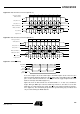
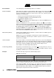
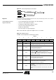
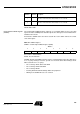
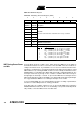
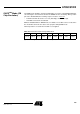
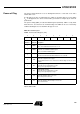
Table Of Contents
- Features
- Description
- Block Diagram
- SFR Mapping
- Pin Configurations
- Oscillators
- Enhanced Features
- Dual Data Pointer Register DPTR
- Expanded RAM (XRAM)
- Reset
- Power Monitor
- Timer 2
- Programmable Counter Array PCA
- Serial I/O Port
- Interrupt System
- Power Management
- Keyboard Interface
- 2-wire Interface (TWI)
- Serial Port Interface (SPI)
- Hardware Watchdog Timer
- ONCE(TM) Mode (ON Chip Emulation)
- Power-off Flag
- EEPROM Data Memory
- Reduced EMI Mode
- Flash Memory
- Electrical Characteristics
- Absolute Maximum Ratings
- DC Parameters
- AC Parameters
- Explanation of the AC Symbols
- External Program Memory Characteristics
- External Program Memory Read Cycle
- External Data Memory Characteristics
- External Data Memory Write Cycle
- External Data Memory Read Cycle
- Serial Port Timing - Shift Register Mode
- Shift Register Timing Waveforms
- External Clock Drive Waveforms
- AC Testing Input/Output Waveforms
- Float Waveforms
- Clock Waveforms
- Ordering Information
- Packaging Information
- Table of Contents
106
AT89C51ID2
4289C–8051–11/05
Reset Value = 00X0 XXXXb
Not Bit addressable
Serial Peripheral DATa Register
(SPDAT)
The Serial Peripheral Data Register (Table 81) is a read/write buffer for the receive data
register. A write to SPDAT places data directly into the shift register. No transmit buffer is
available in this model.
A Read of the SPDAT returns the value located in the receive buffer and not the content
of the shift register.
Table 81. SPDAT Register
SPDAT - Serial Peripheral Data Register (0C5H)
Reset Value = Indeterminate
R7:R0: Receive data bits
SPCON, SPSTA and SPDAT registers may be read and written at any time while there
is no on-going exchange. However, special care should be taken when writing to them
while a transmission is on-going:
• Do not change SPR2, SPR1 and SPR0
• Do not change CPHA and CPOL
• Do not change MSTR
• Clearing SPEN would immediately disable the peripheral
• Writing to the SPDAT will cause an overflow.
1-
Reserved
The value read from this bit is indeterminate. Do not set this bit.
0-
Reserved
The value read from this bit is indeterminate. Do not set this bit.
Bit
Number
Bit
Mnemonic Description
Table 3.
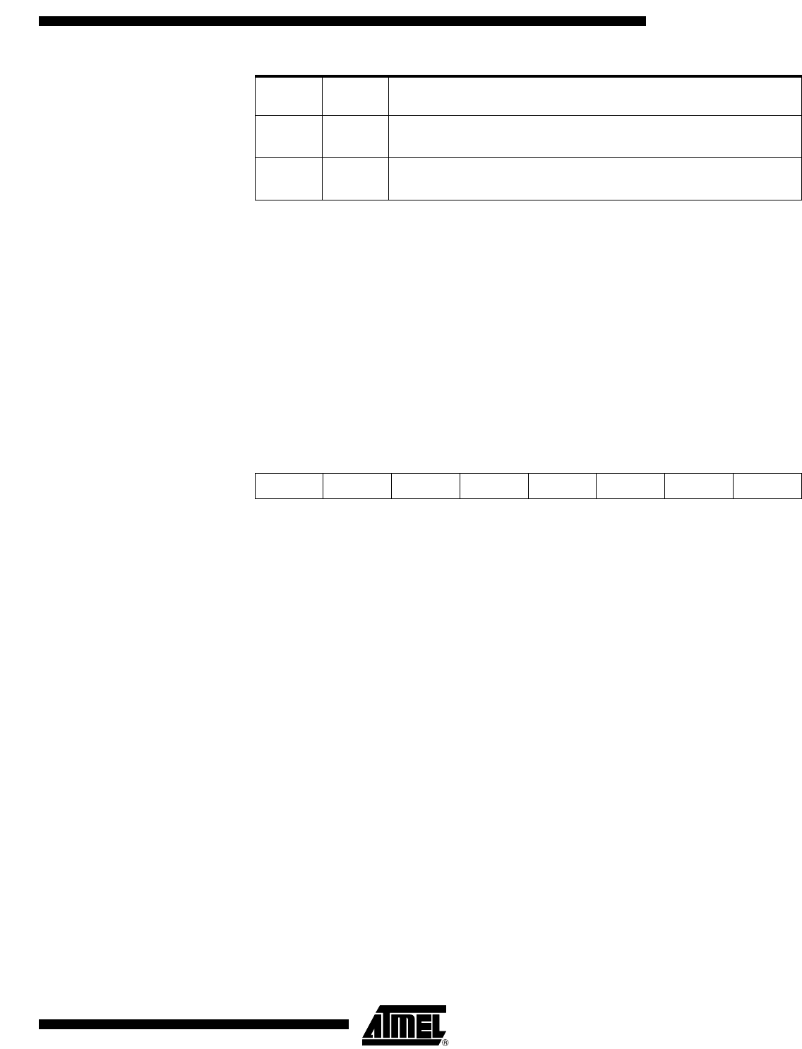
76543210
R7 R6 R5 R4 R3 R2 R1 R0