
User manual

Atmel AVR32025
9
32150B-AVR-03/12
3.1.4.2 Test points
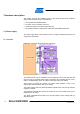
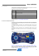
A few test points covering the power supply block have been placed on the Atmel
AT32UC3L-EK for the verification of important signals.
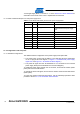
Table 3-2. Power supply block test points.
Designation Feature
TP7 Input voltage level after D1 when the J2 external power supply is used
TP8
Input voltage for all boards’ components except the Atmel AT32UC3L064.
Should be 3.3V nominal
TP9 Input voltage for the AT32UC3L064 VDDIO pin. Should be 3.3V nominal
TP10 Output voltage out of the external regulator
TP11 Input voltage for the AT32UC3L064 VDDIN pin. Should be 3.3V nominal
TP12 GND
To locate the test points mentioned here above, use the assembly top/bottom views
provided in Section 2.4.2, The AT32UC3L-EK schematics.
3.1.5 Power consumption measurement
To
measure the power consumption of the overall board minus the AT32UC3L064,
remove the 0Ω R11 resistor and measure the current over the J4 2-pin header (not
mounted by default).
To measure the power consumption on the AT32UC3L064 VDDIO, remove the 0Ω
R14 resistor and measure the current over the J5 2-pin header (not mounted by
default).
To measure the power consumption on the AT32UC3L064 VDDIN, remove the 0Ω
R19 resistor and measure the current over the J6 2-pin header (not mounted by
default).
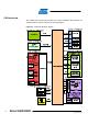
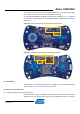
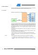
Figure 3-4. AT32UC3L-EK power consumption measurement headers location.
Figure 3-4. AT32UC3L-EK power consum
ption measurement headers location.,”
points to the location of the power consumption measurement area. To accurately
locate the components mentioned here above, use the assembly top/bottom views
provided in Section 2.4.2, The AT32UC3L-EK schematics.