
User manual

Atmel AVR32025
17
32150B-AVR-03/12
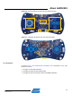
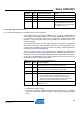
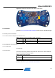
Figure 3-11. Atmel AT32UC3L-EK bottom view external memory location.
3.4.2 Schematics
In Section 2.4.2, The AT32UC3L-EK schematics, the external
memory is described
on page 3.
3.4.3 UC3L-specific information
3.4.3.1 Atm
el AT32UC3L064 pinout for the Atmel DataFlash
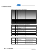
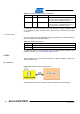
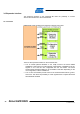
Table 3-10. UC3L pinout for the external memory.
QFP48 pin GPIO GPIO alternate functions Feature
28 PA04 SPI0.MISO DataFlash SO
12 PA05 SPI0.MOSI DataFlash SI
10 PA06 SPI0.SCK DataFlash SCK
15 PA07 SPI0.NPCS DataFlash #CS
22 N.A. N.A. RESET_N pin DataFlash #RESET
3.4.4 Configuration and test points
3.4.4.1 Special consideration when using the DataFlash
The pins PA05, PA06, and PA07 are multiplexed with other components on the
AT32UC3L-EK.
Table 3-11, Conflict conditions with the DataFlash, h
ighlights the components on the
AT32UC3L-EK that might interfere with the DataFlash pins. These components must
not be used while using the DataFlash.