
User manual

14
Atmel AVR32025
32150B-AVR-03/12
3.3.1 Overview
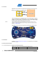
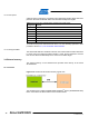
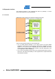
Figure 3-8. Atmel AT32UC3L-EK programming and debugging interface logical view.
The main programming and debugging interface of the AT32UC3L-EK is meant to
program and debug the Atmel AT32UC3L064. There are two debug interfaces
available on the AT32UC3L064: the JTAG interface and the aWire interface (single
pin debug system), both accessible through the J9 connector.
NOTE There is another programming and debugging interface block on the kit, but it is
related to the Atmel AT32UC3B1256 chip in charge of USB communication (refer to
Section 3.7, USB interface).
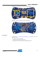
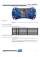
Figure 3-9. AT32UC3
L-EK top view programming and debugging interface location.
3.3.2 Schematics
In Section 2.4.2, The AT32UC3L-EK schematics, the prog
ramming and debugging
interface is on page 5.
3.3.3 UC3L-specific information
3.3.3.1 AT32UC3
L064 pinout for programming and debugging interface
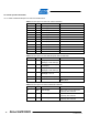
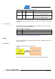
Table 3-7. UC3L pinout for the programming and debugging interface.
QFP48 pin GPIO GPIO alternate functions Feature
11 PA00 None JTAG.TCK