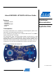
Atmel AVR32025: AT32UC3L-EK User Guide Features • • • • • Kit features overview Kit content Hardware description Schematics Errata 32-bit Atmel Microcontrollers Application Note 1 Introduction The Atmel® AT32UC3L-EK is an evaluation kit and development system for the Atmel AVR® UC3 AT32UC3L064 microcontroller. As an evaluation kit, the board focus is towards Atmel QTouch® and QMatrix support, and picoPower® technology.
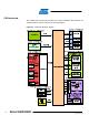
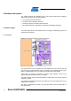
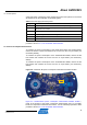
Kit overview This chapter lists the features provided by the Atmel AT32UC3L-EK evaluation kit, and describes the content of the box the kit is packaged in. Figure 2-1. AT32UC3L-EK block diagram.
Atmel AVR32025 2.
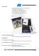
2.2 Kit content The Atmel AT32UC3L-EK toolbox contains the following items: • • • • • • One AVR Technical Library DVD One Atmel AT32UC3L-EK customer letter One Atmel AT32UC3L-EK Getting Started Guide One Atmel AT32UC3L-EK evaluation kit One mini-B plug to std-A plug ~1.5m USB cable One 1.2V NiMh rechargeable battery Figure 2-2. Unpacked AT32UC3L-EK toolbox. 2.3 Power up and getting started Refer to the AVR32777: AT32UC3L-EK Getting Started document. 2.4 References 2.4.
Atmel AVR32025 2.4.4 The 32-bit AVR UC3 L series schematic checklist http://www.atmel.com/dyn/resources/prod_documents/doc32129.pdf 2.4.5 The Atmel AVR Software Framework http://www.atmel.com/asf All pre-loaded firmware source code is available in the AVR Software Framework version 2.0 or higher. 2.4.6 The Atmel AVR UC3 UART boot loader The Atmel UC3L064/32/16 devices are all pre-loaded with a UART boot loader which source code is available in the Atmel Software Framework. 2.4.
3 Hardware description This chapter presents the hardware blocks of the Atmel AT32UC3L-EK hardware design. Each hardware block is described with: • • • • An overview of the hardware block A location in the schematics document AT32UC3L-specific information (when relevant) All possible hardware configurations of the block and available test points 3.1 Power supply The power supply block of the AT32UC3L-EK is in charge of distributing power to all components of the board. 3.1.1 Overview Figure 3-1.
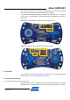
Atmel AVR32025 The “Power Off” signal from the Atmel AT32UC3L064 to the on-board power supply block can be used to lower the power consumption by software. To customize the hardware configuration of this block, see Section 3.1.4.1, Hardware configurations, for a description of the possible hardware configurations of the power supply block. Figure 3-2. Atmel AT32UC3L-EK top view power supply location. Figure 3-3. AT32UC3L-EK bottom view power supply location. 3.1.
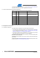
“3.3V Single Supply Mode,” in section 6.1.3.1 in the AVR UC3 L0 Series datasheet for schematics of this mode: this is how it is implemented on this board. 3.1.3.2 Atmel AT32UC3L064 pinout for the power supply block Table 3-1. The Atmel AVR UC3L pinout for the power supply block. QFP48 pin GPIO GPIO alternate functions Feature 1 N.A. N.A. GND 4 PA03 GPIO[3] The Power-Off signal from the AT32UC3L064 to the power supply block 17 N.A. N.A. VDDIN 18 N.A. N.A. VDDCORE 19 N.A. N.A.
Atmel AVR32025 3.1.4.2 Test points A few test points covering the power supply block have been placed on the Atmel AT32UC3L-EK for the verification of important signals. Table 3-2. Power supply block test points. Designation Feature TP7 Input voltage level after D1 when the J2 external power supply is used TP8 Input voltage for all boards’ components except the Atmel AT32UC3L064. Should be 3.3V nominal TP9 Input voltage for the AT32UC3L064 VDDIO pin. Should be 3.
3.2 User interface The main user interface block of the Atmel AT32UC3L-EK covers all components providing a direct interface [visual (output) or tactile (input)] to the user. 3.2.1 Overview Figure 3-5. AT32UC3L-EK user interface logical view. The main user interface offered by the kit is the touch user interface consisting of the wheel sensor and the five button sensors. The touch sensors are implemented using the QMatrix method (X=6, Y=2).
Atmel AVR32025 Figure 3-6. Atmel AT32UC3L-EK top view user interface location. Figure 3-7. AT32UC3L-EK bottom view user interface location. UC3B 3.2.2 Schematics In Section 2.4.
3.2.3 UC3L-specific information 3.2.3.1 Atmel AT32UC3L064 pinout for the user interface block Table 3-3. UC3L pinout for the touch sensors interface.
Atmel AVR32025 3.2.4 Configuration and test points 3.2.4.1 Hardware configuration The default hardware configuration of the user interface block implies that: • There is no hardware to support debounce on the RST pushbutton: R36 is not mounted, so C4 has no effect. This was done to support the aWire programming and debugging interface (refer to Section 3.3 Programming and debugging interface) To enable the hardware debounce support on the RST pushbutton, mount the 0Ω R36 resistor (solder patch).
3.3.1 Overview Figure 3-8. Atmel AT32UC3L-EK programming and debugging interface logical view. The main programming and debugging interface of the AT32UC3L-EK is meant to program and debug the Atmel AT32UC3L064. There are two debug interfaces available on the AT32UC3L064: the JTAG interface and the aWire interface (single pin debug system), both accessible through the J9 connector.
Atmel AVR32025 QFP48 pin GPIO GPIO alternate functions Feature 14 PA01 None JTAG.TMS 13 PA02 None JTAG.TDO 4 PA03 None JTAG.TDI 22 N.A. N.A. RESET_N pin. Used when enabling/disabling the JTAG or the aWire interface. Also, the aWire data is multiplexed on this pin 3.3.4 Configuration and test points 3.3.4.1 Special considerations for the RESET_N pin and the JTAG pins On the Atmel AVR UC3 L0 series, the RESET_N pin is used to enable/disable the JTAG interface or the aWire interface.
3.3.4.2 Test points A few test points covering the programming and debugging interface block have been placed on the Atmel AT32UC3L-EK for the verification of important signals. Table 3-9. Programming and debugging interface block test points. Designation Feature TP24 JTAG.TCK TP25 JTAG.TDO TP26 JTAG.TMS TP27 JTAG.TDI TP28 GND TP29 VCC3 TP30 RESET_N To locate the test points mentioned here above, use the assembly top/bottom views provided in Section 2.4.2, The AT32UC3L-EK schematics. 3.3.4.
Atmel AVR32025 Figure 3-11. Atmel AT32UC3L-EK bottom view external memory location. 3.4.2 Schematics In Section 2.4.2, The AT32UC3L-EK schematics, the external memory is described on page 3. 3.4.3 UC3L-specific information 3.4.3.1 Atmel AT32UC3L064 pinout for the Atmel DataFlash Table 3-10. UC3L pinout for the external memory. QFP48 pin GPIO GPIO alternate functions Feature 28 PA04 SPI0.MISO DataFlash SO 12 PA05 SPI0.MOSI DataFlash SI 10 PA06 SPI0.SCK DataFlash SCK 15 PA07 SPI0.
Table 3-11. Conflict conditions with the DataFlash. QFP48 pin GPIO DataFlash signal Conflict conditions 28 PA04 DataFlash SO If the WLESS J8 connector is configured with a jumper on J44.2-4, signal activities over J8.2 will conflict with the DataFlash SO signal 12 PA05 If the WLESS J8 connector is configured with a jumper on J44.1-3, signal activities over J8.
Atmel AVR32025 Figure 3-13. AT32UC3L-EK bottom view 32kHz crystal location. 3.5.2 Schematics In Section 2.4.2, The AT32UC3L-EK schematics, the RTC block is described on page 1. 3.5.3 UC3L-specific information 3.5.3.1 Atmel AT32UC3L064 pinout for the RTC block Table 3-13. UC3L pinout for the 32kHz crystal connections. QFP48 pin GPIO GPIO alternate functions Feature 26 PA13 N.A. XIN32_2 Crystal 32kHz input 25 PA20 N.A. XOUT32_2 Crystal 32kHz output 3.5.4 Configuration and test points 3.5.4.
3.6 Expansion interface The expansion interface on the AT32UC3L-EK offers the possibility to connect various external devices to the AT32UC3L064. 3.6.1 Overview Figure 3-14. Atmel AT32UC3L-EK expansion interface logical view. There are two expansion headers on the AT32UC3L-EK: • The J8 header (labeled WLESS on the PCB) connects the Atmel RZ600 AT86RF231 radio board to provide wireless communication capabilities to the kit. Signals on J8.1 and J8.2 are configurable with the J44 header.
Atmel AVR32025 Figure 3-15. AT32UC3L-EK top view expansion headers location. 3.6.2 Schematics In Section 2.4.2, The AT32UC3L-EK schematics, the expansion headers are described: • On page 4 for the wireless J8+J44 headers • On page 7 for the J14 and J15 headers 3.6.3 UC3L-specific information 3.6.3.1 Atmel AT32UC3L064 pinouts for the expansion headers Table 3-15. UC3L pinouts for the J8 and J44 headers. QFP48 pin GPIO GPIO alternate functions Feature 11 PA00 USART1.
QFP48 pin GPIO GPIO alternate functions Feature 12 PA05 TWI0.TWD Provides access to the TWI0 TWD signal. Available on J8.1 if J44 is configured with a jumper connecting J44.1 to J44.3 10 PA06 SPI0.SCK RZ600 SPI clock. Available on J8.8 3 PA08 USART1.TX or GPIO[8] Provides access to the RZ600.SLP_TR feature or to the USART1.TX signal. Available on J8.4 2 PA09 USART1.RX or GPIO[9] Provides access to the RZ600.IRQ feature or to the USART1.RX signal. Available on J8.3 N.A. N.A. N.A. GND.
Atmel AVR32025 QFP48 pin GPIO GPIO alternate functions Feature 24 PA21 Software-dependant J15.7 9 PA22 Software-dependant J15.9 6 PB00 Software-dependant J15.11 16 PB01 Software-dependant J15.13 7 PB02 Software-dependant J15.15 8 PB03 Software-dependant J15.17 - - - GND on J15.19 - - - VCC3 on J15.2 21 PB04 Software-dependant J15.4 20 PB05 Software-dependant J15.6 30 PB06 Software-dependant J15.8 31 PB07 Software-dependant J15.
3.7.1 Overview Figure 3-16. Atmel AT32UC3L-EK USB interface logical view. The USB interface provides two features to the AT32UC3L-EK kit: • USB communication • Power supply (see Section 3.1, Power supply for a description of that feature) The USB controller is the Atmel AT32UC3B1256. The AT32UC3B1256 comes pre-loaded with several firmware components: • A USB DFU boot loader [accessible upon power up when the J12 header is closed (see Figure 3-17. Atmel AT32UC3L-EK top view USB interface location.
Atmel AVR32025 • Two LEDs, D12 and D13, [with the default firmware (except the USB DFU boot loader) these LEDs are blinking, depending on the activity over the USB] • The USB MODE pushbutton on the PCB. With the default pre-loaded firmware, this button is used at power up to choose between the virtual com port firmware or the HID QTouch Debug firmware (see Section 3.7.4.
Figure 3-18. Atmel AT32UC3L-EK bottom view USB interface location. J13 UC3B 3.7.2 Schematics In Section 2.4.2, The AT32UC3L-EK schematics, the USB interface block is described on page 6. 3.7.3 UC3L-specific information 3.7.3.1 Atmel T32UC3L064 pinout for the USB interface block Table 3-18. UC3L pinout for the USB interface block. QFP48 pin GPIO GPIO alternate functions Feature 6 PB00 USART3.TXD USART3 TX line 16 PB01 USART3.RXD USART3 RX line 3.7.4 Configuration and test points 3.7.4.
Atmel AVR32025 Table 3-19. USB interface block test points. Designation Feature TP31 VBUS TP32 D- TP33 D+ TP34 GND TP35 JTAG.TCK.UC3B TP36 JTAG.TDO.UC3B TP37 JTAG.TMS.UC3B TP38 JTAG.TDI.UC3B TP39 RESET_N.UC3B TP41 USB MODE pushbutton state To locate the test points mentioned here above, use the assembly top/bottom views provided in Section 2.4.2, The AT32UC3L-EK schematics. 3.8 Atmel AT32UC3L064 The AT32UC3L064 is the central point of the Atmel AT32UC3L-EK. 3.8.
The expansion interface offers the possibility to connect various external devices to the Atmel AT32UC3L064. The J8 header (labeled WLESS on the PCB) connects an Atmel RZ600 AT86RF231 radio board (not provided with this board) to provide wireless capabilities to the kit. Obviously, dedicated firmware must be running on the AT32UC3L064 to support this feature. The J14 and J15 headers provide access to all of the AT32UC3L064’s GPIOs. For a detailed presentation of the expansion interface block, see Section 3.
Atmel AVR32025 QFP48 Pin GPIO GPIO alternate functions Feature 48 N.A. N.A. VDDIO 42 N.A. N.A. VDDIO 11 PA00 JTAG.TCK / USART1.RTS / GPIO[0] JTAG_TCK / WZ_U1_RTS / WZ_RZ600_RST 14 PA01 JTAG.TMS / USART1.CTS / GPIO[1] JTAG_TMS / WZ_U1_CTS / WZ_RZ600_MISC 13 PA02 JTAG.TDO JTAG TDO 4 PA03 JTAG.TDI / GPIO[3] / SPI.NPCS[1] JTAG_TDI / POWER_OFF / WZ_RZ600_CS 28 PA04 SPI.MISO / TWIMS0.TWCK DF_MISO / WZ_MISO / WZ_TW0CK 12 PA05 SPI.MOSI / TWIMS0.
NOTE QFP48 Pin GPIO GPIO alternate functions Feature 23 PB10 GPIO[42] / GLOC.OUT[1] / PWAM[33] LED_1 44 PB11 CAT.VDIVEN CAT-VDIVEN 5 PB12 CAT.CSA[15] TOUCH_Y7 Some pins offer multiple GPIO alternate function configuration, while others don’t. For example, for LED1 (PB10), it is possible to drive the intensity of the LED through a regular GPIO function or through the PWMA function multiplexed on this pin. However, for TOUCH_Y7 (PB12), if the GPIO function configuration is different than CAT.
Atmel AVR32025 4 Schematics and assembly top/bottom views See Section 2.4.2.
5 Errata 5.1 While using the touch sensors, if the bottom side is touched, the touch events are wrong Workaround: when demonstrating the touch feature on the kit, the bottom side of the PCB must not be in contact with fingers or any external object. 5.2 The pin-through holes near the touch sensors may cause spurious touch events On some Atmel AT32UC3L-EK kits, the pin-through holes are not protected, causing spurious touch events when the fingers are not exactly on the touch sensors.
Atmel AVR32025 6 Evaluation board/kit – important notice This evaluation board/kit is intended for use for FURTHER ENGINEERING, DEVELOPMENT, DEMONSTRATION, OR EVALUATION PURPOSES ONLY. It is not a finished product and may not (yet) comply with some or any technical or legal requirements that are applicable to finished products, including, without limitation, directives regarding electromagnetic compatibility, recycling (WEEE), FCC, CE or UL (except as may be otherwise noted on the board/kit).
7 Table of contents Features ............................................................................................... 1 1 Introduction ...................................................................................... 1 2 Kit overview...................................................................................... 2 2.1 Features .............................................................................................................. 3 2.2 Kit content.....................................
Atmel AVR32025 3.6.1 Overview ................................................................................................................. 20 3.6.2 Schematics.............................................................................................................. 21 3.6.3 UC3L-specific information ....................................................................................... 21 3.6.4 Configuration and test points.............................................................................
Atmel Corporation 2325 Orchard Parkway San Jose, CA 95131 USA Tel: (+1)(408) 441-0311 Fax: (+1)(408) 487-2600 www.atmel.com Atmel Asia Limited Unit 01-5 & 16, 19F BEA Tower, Milennium City 5 418 Kwun Tong Road Kwun Tong, Kowloon HONG KONG Tel: (+852) 2245-6100 Fax: (+852) 2722-1369 Atmel Munich GmbH Business Campus Parkring 4 D-85748 Garching b. Munich GERMANY Tel: (+49) 89-31970-0 Fax: (+49) 89-3194621 Atmel Japan 16F, Shin Osaki Kangyo Bldg.