
User manual

22
AVR32919
32151A-AVR-09/10
4.5.2 UC3C-Specific Information
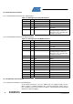
4.5.2.1 AT32UC3C0512C pinout for the JTAG Interface
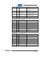
Table 4-13. UC3C pinout for the JTAG interface
QFP144 pin GPIO GPIO alternate function Feature
1 PA00 None JTAG.TCK
2 PA01 None JTAG.TDI
3 PA02 None JTAG.TDO
4 PA03 None JTAG.TMS
142 N.A. N.A.
RESET_N pin. Used when
enabling/disabling the JTAG or the
aWire interface. Also, the aWire data
is multiplexed on this pin
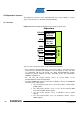
4.5.2.2 AT32UC3C0512 pinout for the NEXUS Interface
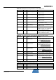
Table 4-14. UC3C pinout for the NEXUS interface
QFP144 pin GPIO GPIO alternate function Feature
1 PA00 None JTAG.TCK
2 PA01 None JTAG.TDI
3 PA02 None JTAG.TDO
4 PA03 None JTAG.TMS
142 N.A. N.A.
RESET_N pin. Used when
enabling/disabling the JTAG or the
aWire interface. Also, the aWire data
is multiplexed on this pin
27 PA10 N.A. EVTI_N
9 PB06 N.A. MDO[5]
18 PB15 N.A. MDO[4]
17 PB14 N.A. MDO[3]
46 PA27 N.A. MDO[2]
45 PA26 N.A. MDO[1]
36 PA19 N.A. MDO[0]
138 PD29 N.A. EVTO_N
65 PB26 N.A. MCKO
64 PB25 N.A. MSEO[1]
57 PB18 N.A. MSEO[0]
4.5.3 Configuration and Test Points
4.5.3.1 Special Considerations for the NEXUS pins
On the Atmel AVR UC3 C series, the NEXUS pins are multiplexed with I/O lines.
While using these multiplexed NEXUS lines all normal peripheral activity on these
lines is disabled. The user must make sure that no external peripheral is blocking the
NEXUS lines while debugging.