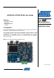
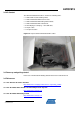
AVR32919: AT32UC3C-EK User Guide Features • • • • Kit Features Overview Kit Content Hardware Description Schematic 8-bit Microcontrollers Application Note 1 Introduction The Atmel® AT32UC3C-EK is an evaluation kit and development system for the Atmel AVR® UC3 AT32UC3C0512C microcontroller. As a development system, the board notably provides on-board memory, a USB communication interface, CAN and LIN network interfaces and the JTAG programming and debugging interface.
Abbreviations ASF: AVR Software Framework CAN: Controlled Area Network LIN: Local Interconnect Network HMI: Human Machine Interface 2 AVR32919 32151A-AVR-09/10
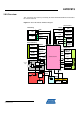
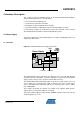
AVR32919 3 Kit Overview This section lists the features provided by the Atmel AT32UC3C-EK kit and describes the content of the kit. Figure 3-1. Atmel AT32UC3C-EK Block Diagram User Interface Networking DACIFB Audio Jack (J22) ADCIFA Mic. (U21) Pot.
3.1 Features This section lists the main components and interfaces of the Atmel AT32UC3C-EK kit: • Main MCU: 32-bit Atmel AVR UC3 AT32UC3C0512C (TQFP144) o 512 Kbytes internal Flash, 256 Kbytes internal RAM o Up to 66 MHz operations o Controller Area Network Interfaces o Peripheral Event System o FlashVault™ allows pre-programmed Secure library support for enduser applications o DSP Floating Point Instructions. • Powered through USB connector or through external power supply (header J1 or J2).
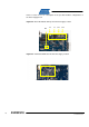
AVR32919 3.2 Kit Content The Atmel AT32UC3C-EK toolbox contains the following items: • • • • • • • 1x Atmel AVR Technical Library DVD, 1x Atmel AT32UC3C-EK Customer letter, 1x Atmel AT32UC3C-EK Getting Started Guide, 1x Atmel AT32UC3C-EK evaluation kit, 2x mini-B plug to std-A plug ~1.5m USB cable, 5x 2-pins cable, 1x 10-pins flat cable. Figure 3-2. Unpacked Atmel AT32UC3C-EK Toolbox 3.3 Power-up and getting started Refer to the “AT32UC3C-EK Getting Started Document” included in the kit. 3.
3.4.4 The AVRMC300 Getting Started http://www.atmel.com/dyn/products/tools_card.asp?tool_id=4374 3.4.5 The 32-bit AVR UC3 C Series Schematic Checklist http://www.atmel.com/dyn/products/app_notes.asp?family_id=607 3.4.6 The AVR Software Framework http://asf.atmel.no/readme.html All pre-loaded firmware source codes are available in the AVR Software Framework version 2.0 or higher. 3.4.7 Debuggers http://www.atmel.com/dyn/products/tools.
AVR32919 4 Hardware Description This section presents the hardware blocks of the Atmel AT32UC3C-EK hardware design. Each hardware block is described with: • an overview of the hardware block, • a location in the schematics document, • AT32UC3C-specific information (when relevant), • all possible hardware configurations of the block and available test points. In each block description, the components reference and schematic can be found in The AT32UC3C-EK Schematics and Assembly bottom/ top view 4.
Refer to section 4.1.3.1 for a description of the possible hardware configurations of the Power Supply block. Figure 4-2. Atmel AT32UC3C-EK Top View Power Supply Location D3 J2 J1 J21 J27 Figure 4-3.
AVR32919 4.1.2 UC3C-Specific Information 4.1.2.1 AT32UC3C0512C Power Supply Mode Among the two power supply configurations supported by the Atmel AT32UC3C0512C, this board implements the 3.3V Single Supply Mode configuration. Refer to the Figure “3.3V Single Supply mode” of the Power Considerations section in the AVR UC3 C0 Series datasheet for schematic diagram of this mode. 4.1.2.2 AT32UC3C0512C pinout for the Power Supply Block Table 4-1.
4.1.3.2 Test Points A few test points covering the Power Supply block have been placed on the Atmel AT32UC3C-EK for the verification of important signals. Table 4-2. Power Supply block Test Points Designation Feature TP12-14 Input voltage level after D1 when the J1 external Power Supply is used TP20-21 Input voltage level after D2 when the J2 external Power Supply is used TP22-23 Input voltage for 3.3V regulator. 5V nominal TP24-25 Input voltage for all board components. 3.
AVR32919 Figure 4-4.
4.2 User Interface The main User Interface block of the AT32UC3C-EK features all components providing a HMI (visual (output) or tactile (input)) to the user. 4.2.1 Overview Figure 4-5.
AVR32919 Figure 4-6. Atmel AT32UC3C-EK Top View User Interface Location LCD + touch screen Audio Jack (J22) Reset Button Capacitive touch sensors Microphone Push buttons Potentiometer (P1) LEDs Figure 4-7. AT32UC3C-EK Bottom View User Interface Location Capacitive touch controller 4.2.2 UC3C-Specific Information 4.2.2.1 AT32UC3C0512C pinout for the User Interface block Table 4-3.
Table 4-4. UC3C pinout for the LEDs and push-buttons interfaces QFP144 pin GPIO GPIO alternate function Feature 25 PA8 GPIO[8] LED0 132 PD23 GPIO[119] LED1 86 PC13 GPIO[77] or PWMH[2] LED2 131 PD22 GPIO[118] or TC0-A2 LED3 31 PA14 GPIO[14] PB0 push-button 48 PA29 GPIO[29] or EXTINT[0] PB1 push-button N.A. N.A. RST push-button, connected to the RESET_N pin Table 4-5.
AVR32919 4.2.3 Configuration & Test Points 4.2.3.1 Hardware Configuration The default hardware configuration of the User Interface block connects the QVGA LCD Display is connected through parallel interface (with EBI). To switch to the serial interface (with SPI): • Remove the 0 Ohm R44 and R52 resistors. • Mount the 0 Ohm R48 and R54 resistors. 4.2.3.2 Test Points A few test points covering the User Interface block have been placed on the Atmel AT32UC3C-EK for the verification of important signals.
4.3 Networking The networking block of the AT32UC3C-EK covers all components providing CAN and LIN bus interfaces through DB9 connectors and 3-pins headers. 4.3.1 Overview Figure 4-8. Atmel AT32UC3C-EK Networking Logical View The networking block supports both CAN and LIN interface: 16 • The CAN transceivers are embedded on the UC3C-EK (U9 and U11) and termination resistors can be used as bus configuration through 2-pin headers (J9 and J14). See 4.1.3.1 section.
AVR32919 Figure 4-9. AT32UC3C-EK Top View Networking Location J15 J10 J18 J13 4.3.2 UC3C-Specific Information 4.3.2.1 AT32UC3C0512C pinout for the User Interface block Table 4-7. UC3C pinout for the CAN interface QFP144 pin GPIO GPIO alternate function Feature 36 PB04 RX CAN0 RX CAN 37 PB05 TX CAN0 TX CAN 84 PC11 RX CAN1 RX CAN 85 PC12 TX CAN1 TX CAN Table 4-8.
by the LIN bus. To suppress this feature, remove jumpers on the 2-pins headers (J11 or J16). 4.4 External Memory The External Memory on the Atmel AT32UC3C-EK provides extra memory to the Atmel AT32UC3C0512C. 4.4.1 Overview Figure 4-10.
AVR32919 Figure 4-11. AT32UC3C-EK Bottom View External Memory Location SDRAM (U6) Dataflash (U5) SD/MMC (J7) EEPROM (U8) 4.4.2 UC3C-Specific Information 4.4.2.1 AT32UC3C0512 pinout for the Atmel EEPROM Table 4-9. UC3C pinout for the External Memory QFP144 pin GPIO GPIO Function Feature 73 PC02 TWIMS0_TWD TWI Data 74 PC03 TWIMS0_TWCK TWI Clock 4.4.2.2 AT32UC3C0512 pinout for the Atmel DataFlash Table 4-10.
4.4.2.3 AT32UC3C0512 pinout for the SD/MMC Slot Table 4-11. UC3C pinout for the External Memory QFP144 pin GPIO GPIO alternate function Feature 58 PB19 SPI1.MISO SD SO 59 PB20 SPI1.MOSI SD SI 60 PB21 SPI1.SCK SD SCK 61 PB22 SPI1.NPCS3 SD #CS 139 PD30 GPIO[28] SD Write Protect 47 PA28 GPIO[126] SD Card Protect 4.4.2.4 AT32UC3C0512 pinout for the SDRAM Table 4-12.
AVR32919 4.5 Programming & Debugging Interface The Programming & Debugging Interface block of the Atmel AT32UC3C-EK provides the developer a mean to debug an application running on the Atmel AT32UC3C0512C. 4.5.1 Overview Figure 4-12. Atmel AT32UC3C-EK Programming & Debugging Interface Logical View Trace Debug JTAG+ Awire (J9) NEXUS (J23) The main Programming and Debugging Interface of the AT32UC3C-EK is meant to program and debug the Atmel AT32UC3C0512C.
4.5.2 UC3C-Specific Information 4.5.2.1 AT32UC3C0512C pinout for the JTAG Interface Table 4-13. UC3C pinout for the JTAG interface QFP144 pin GPIO GPIO alternate function Feature 1 PA00 None JTAG.TCK 2 PA01 None JTAG.TDI 3 PA02 None JTAG.TDO 4 PA03 None JTAG.TMS 142 N.A. N.A. RESET_N pin. Used when enabling/disabling the JTAG or the aWire interface. Also, the aWire data is multiplexed on this pin 4.5.2.2 AT32UC3C0512 pinout for the NEXUS Interface Table 4-14.
AVR32919 Table 4-15 highlights the components of the Atmel AT32UC3C-EK that might interfere with the multiplexed NEXUS pins. These components must not be used while debugging with the NEXUS interface. Table 4-15.
4.6 Expansions Interface The Expansions interface on the AT32UC3C-EK offers the possibility to connect various external devices to the Atmel AT32UC3C0512C. 4.6.1 Overview Figure 4-14.
AVR32919 • Refer to section 3.4.4 for more detailed information. Figure 4-15. Atmel AT32UC3C-EK Top View Expansion Headers Location AVRMC300 Expansion headers J33 J19+J20 J25+J44 J43 4.6.2 UC3C-Specific Information 4.6.2.1 AT32UC3C0512C pinout for the Expansion Interfaces Table 4-17. UC3C pinout for the J25 and J44 headers 32151A-AVR-09/10 QFP144 pin GPIO GPIO alternate function Feature 17 PB14 USART1.RTS Provides access to the USART1.RTS signal. Available on J25.
QFP144 pin GPIO GPIO alternate function Feature 73 PC02 TWIMS0.TWD Provides access to the TWIMS0 TWD signal. Available on J25.1 if J44 is configured with a jumper connecting J44.1 to J44.3 60 PB21 SPI1.SCK WLESS SPI clock. Available on J25.8 19 PB16 USART1.TX Provides access to the USART1.TX signal. Available on J25.4 20 PB17 USART1.RX Provides access to the USART1.RX signal. Available on J25.3 N.A. N.A. N.A. GND. Available on J25.9 N.A. N.A. N.A. VCC3. Available on J25.
AVR32919 Table 4-20. UC3C pinout for the power drives control signal (J33) QFP144 pin GPIO GPIO alternate function Feature 12 PB9 PWM-PWMH[0] Provides access to the PWM UH signal available on J33.1 11 PB8 PWM-PWML[0] Provides access to the PWM UL signal available on J33.2 14 PB11 PWM-PWMH[1] Provides access to the PWM VH signal available on J33.3 13 PB10 PWM-PWML[1] Provides access to the PWM VL signal available on J33.
Table 4-23. UC3C pinout for the hall sensors (J43) QFP144 pin GPIO GPIO alternate function Feature 66 PB27 QDEC – QEPA Quadrature Decoder Line A 67 PB28 QDEC – QEPB Quadrature Decoder Line B 68 PB29 QDEC – QEPI Quadrature Decoder Line I - - - GND on J43.5 - - - VCC3 on J43.1 4.6.3 Configuration and Test Points 4.6.3.1 Configuration The J25.1 and J25.2 pins are configurable through the J44 header. Refer to Table 417, for a description of the possible configurations. 4.6.3.
AVR32919 4.7 USB Virtual Com Port Interface The USB Virtual Com Port interface on the Atmel AT32UC3C-EK offers USB CDC Serial Com Port communication capabilities to the Atmel AT32UC3C0512C through the on-board Atmel AT32UC3B1256 device. 4.7.1 Overview Figure 4-16.
Figure 4-17. Atmel AT32UC3C-EK Top View USB Virtual Com Port Interface Location J27 J31 4.7.2 UC3C-Specific Information 4.7.2.1 AT32UC3C0512C pinout for the USB Virtual Com Port Interface block Table 4-24. UC3C pinout for the USB Virtual Com Port Interface block QFP144 pin GPIO GPIO alternate function Feature 78 PC05 USART2.RXD USART2 RX line 77 PC04 USART2.TXD USART2 TX line 4.7.3 Configuration & Test Points 4.7.3.
AVR32919 4.7.3.2 Test Points A few test points covering the USB Interface block have been placed on the Atmel AT32UC3C-EK for the verification of important signals. Table 4-25. USB Interface block Test Points 32151A-AVR-09/10 Designation Feature TP64 VBUS TP65 D- TP66 D+ TP67 GND TP68 JTAG.TCK.UC3B TP69 JTAG.TDO.UC3B TP70 JTAG.TMS.UC3B TP71 JTAG.TDI.UC3B TP72 RESET_N.
4.8 USB Interface The USB interface on the AT32UC3C-EK demonstrates the USB device and embedded host communication capabilities of the Atmel AT32UC3C0512C. 4.8.1 Overview Figure 4-18. AT32UC3C-EK USB Interface Logical View The USB interface provides two features to the AT32UC3C-EK kit: • USB communication. • Power supply (see section 4.1 for a description of that feature) in USB device mode.
AVR32919 Figure 4-19. Atmel AT32UC3C-EK Top View USB Interface Location J21 USB Device Mode Power Supply 4.8.2 UC3C-Specific Information 4.8.2.1 AT32UC3C0512C pinout for the USB Interface block Table 4-26.
4.8.3 Configuration 4.8.3.1 Bootloader A USB DFU Bootloader is pre-loaded on the Atmel AT32UC3C0512C. To enter this bootloader mode, the PB0 push-button must be pressed upon reset, then released. It is then possible to program the AT32UC3C0512C through the USB DFU Bootloader (see App note http://www.atmel.com/dyn/products/app_notes.asp?family_id=607) . Figure 4-20. Atmel AT32UC3C-EK Top View USB Bootloader Interface Location USB DFU Connector PB0 4.8.3.
AVR32919 4.9 AT32UC3C0512C The Atmel AT32UC3C0512C is the central point of the Atmel AT32UC3C-EK. 4.9.1 Overview See Figure 3-1 for a logical view representing a logical view of the AT32UC3C0512C in the kit. The AT32UC3C0512C is powered from the Power Supply block. For a detailed presentation of the Power Supply block, see section 4.1.
Programming & Debugging Interface. The AT32UC3C0512C has access to: • • • • 1x external on-board Atmel DataFlash 64 Mbit memory. 1x external on-board Atmel EEPROM 128-bits memory. 1x external on-board SDRAM 256 Mbits memory. 1x external on-board SD/MMC slot. For a detailed presentation of the External Memory block, see section 4.4. 4x networking interfaces available on AT32UC3C0512C are accessible: • 2x CAN Interfaces. • 2x LIN Interfaces.
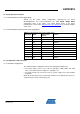
AVR32919 QFP144 pin GPIO GPIO alternate function Feature 53 N.A. N.A. VDDIN5 54 N.A. N.A. VDDIN33 52 N.A. N.A. GNDPLL 55 N.A. N.A. VDDCORE 56 N.A N.A GNDCORE 37 N.A. N.A. GNDANA 34-35 N.A. N.A. ADCREFP/N 38 N.A. N.A. VDDANA 5-76-104-119 N.A. N.A GNDVDDIO 5-75-103-118 N.A. N.A. VDDIO N.A. N.A. RST push-button, connected to the RESET_N pin 1 PA00 None JTAG.TCK 2 PA01 None JTAG.TDI 3 PA02 None JTAG.TDO 4 PA03 None JTAG.TMS Table 4-28.
QFP144 pin GPIO GPIO alternate function Feature 43 PA24 ADCIFA-ADCIN13 TFT XR Line Measurement 44 PA25 ADCIFA-ADCIN14 Microphone Input 45 PA26 N.A MDO[1] 46 PA27 N.A MDO[2] 47 PA28 GPIO[126] SD Card Protect 48 PA29 GPIO[29] or EXTINT[0] PB1 push-button Table 4-29. UC3C pinout Port B 38 QFP144 pin GPIO GPIO alternate function Feature 140 PB00 Xin0 141 PB01 Xout0 142 PB02 Xin1 143 PB03 Xout1 36 PB04 RX CAN0 RX CAN 37 PB05 TX CAN0 TX CAN 9 PB06 N.
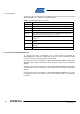
AVR32919 QFP144 pin GPIO GPIO alternate function Feature 58 PB19 SPI1.MISO Dataflash SO / SD SO / WLESS.MOSI / TFT Interface through the SPI 59 PB20 SPI1.MOSI Dataflash SI / SD SI / WLESS.MISO / TFT Interface through the SPI 60 PB21 SPI1.SCK Dataflash SCK / SD SCK / WLESS SPI clock / TFT Interface through the SPI 61 PB22 SPI1.NPCS3 SD #CS 62 PB23 SPI1.NPCS2 TFT SPI #CS 63 PB24 SPI1.NPCS1 Dataflash #CS 64 PB25 N.A / SPI1.NPCS[] MSEO[1] 65 PB26 N.
QFP144 pin GPIO GPIO alternate function Feature 90 PC17 EBI RASn SDRAM RASn 91 PC18 EBI SDA10 SDRAM SDA10 92 PC19 EBI-D0 TFT Data Bus 93 PC20 EBI-D1 TFT Data Bus 94 PC21 EBI-D2 TFT Data Bus 95 PC22 EBI-D3 TFT Data Bus 96 PC23 EBI-D4 TFT Data Bus 97 PC24 EBI-D5 TFT Data Bus 98 PC25 EBI-D6 TFT Data Bus 99 PC26 EBI-D7 TFT Data Bus 100 PC27 EBI-D8 / Softwaredependant TFT Data Bus / J19.9 101 PC28 EBI-D9 / Softwaredependant TFT Data Bus / J19.
AVR32919 QFP144 pin GPIO GPIO alternate function Feature 115 PD8 EBI A4 SDRAM Address Bus 116 PD9 EBI A5 SDRAM Address Bus 117 PD10 EBI A6 SDRAM Address Bus 120 PD11 EBI A7 SDRAM Address Bus 121 PD12 EBI A8 SDRAM Address Bus 122 PD13 EBI SDCK SDRAM Clock 123 PD14 EBI A10 SDRAM Address Bus 124 PD15 EBI A11 / Softwaredependant SDRAM Address Bus / J20.6 125 PD16 EBI-A12/ Softwaredependant TFT Reset Signal / J20.
5 EVALUATION BOARD/KIT – IMPORTANT NOTICE This evaluation board/kit is intended for use for FURTHER ENGINEERING, DEVELOPMENT, DEMONSTRATION, OR EVALUATION PURPOSES ONLY. It is not a finished product and may not (yet) comply with some or any technical or legal requirements that are applicable to finished products, including, without limitation, directives regarding electromagnetic compatibility, recycling (WEEE), FCC, CE or UL (except as may be otherwise noted on the board/kit).
Disclaimer Headquarters International Atmel Corporation 2325 Orchard Parkway San Jose, CA 95131 USA Tel: 1(408) 441-0311 Fax: 1(408) 487-2600 Atmel Asia Unit 1-5 & 16, 19/F BEA Tower, Millennium City 5 418 Kwun Tong Road Kwun Tong, Kowloon Hong Kong Tel: (852) 2245-6100 Fax: (852) 2722-1369 Atmel Europe Le Krebs 8, Rue Jean-Pierre Timbaud BP 309 78054 Saint-Quentin-enYvelines Cedex France Tel: (33) 1-30-60-70-00 Fax: (33) 1-30-60-71-11 Atmel Japan 9F, Tonetsu Shinkawa Bldg.