
User manual


Hardware Specification
© 2008 Microchip Technology Inc. DS51616B-page 119
12.7 HIGH-SPEED COMMUNICATION HARDWARE
For high-speed emulator communication with a target (Section 2.3.2 “High-Speed
Communication”), use the Performance Pak. The Performance Pak includes:
• a High-Speed Driver Board
• a High-Speed Receiver Board
• LVDS Cables
To use this type of communication with a header board, you will need a device-specific
Processor Pak, which includes an 8-pin connector header board containing the desired
ICE/ICD device and a standard adapter board (8-pin to 6-pin connection.)
For more on available header boards, see the “Header Board Specification”
(DS51292).
12.7.1 High-Speed Driver Board
The high-speed driver board consists of two separate multipoint LVDS (Low Voltage
Differential Signal) transmitters and receivers for clock and data. Multipoint LVDS
requires 100 ohm terminations at each driver output and receiver input, per the
standard, and multipoint configurations type 2 receivers are used, as these are
intended for control signals or where fail-safe provisions are needed. Even though the
standard allows for any combination of drivers, receivers and/or transceivers of up to
32 on the line, only two will be used. The driver board has a port expansion which is
controlled by an I
2
C™ interface for sending/receiving status information to/from the
emulator. The high-speed driver board assembly is inserted into the emulator pod via
the card guide.
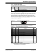
FIGURE 12-4: DUAL 8-PIN PINOUT
Note: You will not need the standard adapter board for high-speed communica-
tions. Instead, you will plug the 8-pin connector end of the high-speed
receiver board directly into the 8-pin connector of the header board.
Note: Data rates up to 40 MIPS are possible.
2
1
4
3
6
5
Bottom of
Receiver Board
2
1
4
3
6
5
J3
J2
J3 Pinout
* Optional - see Section 2.5.2 “SPI Trace Connections (High-Speed
Communication Only)”.
J2 Pinout
Pin Name Function Pin Name Function
1 DATAEN+ Std Data Enable + 5 USPID– *Serial Data –
2 DATAEN– Std Data Enable – 6 CLKEN– Std Clock Enable –
3 CLKEN+ Std Clock Enable + 7 USPIC+ *Serial Clock +
4 USPID+ *Serial Data + 8 USPIC– *Serial Clock –
Pin Name Function Pin Name Function
1 LVC+ LV Std Data + 5 GND Ground
2 LVD– LV Std Data – 6 LVC– LV Std Clock –
3 LVC+ LV Std Clock + 7 V
DD_TGT VDD on target
4V
DD Power 8 VPP_TGT VPP on target
8
7
8
7