
Data Sheet

1998-2021 Microchip Technology Inc. DS20001203X-page 7
24AA256/24LC256/24FC256
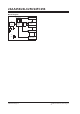
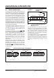
2.0 PIN DESCRIPTIONS
The descriptions of the pins are listed in Table 2-1.
2.1 A0, A1, A2 Chip Address Inputs
The A0, A1 and A2 inputs are used by the 24XX256 for
multiple device operations. The levels on these inputs
are compared with the corresponding bits in the client
address. The chip is selected if the compare is true.
Up to eight devices (two for the MSOP package) may
be connected to the same bus by using different Chip
Select bit combinations. These inputs must be
connected to either V
CC or VSS.
In most applications, the chip address inputs A0, A1
and A2 are hard-wired to logic 0 or logic 1. For
applications in which these pins are controlled by a
microcontroller or other programmable device, the chip
address pins must be driven to logic 0 or logic 1
before normal device operation can proceed.
2.2 Serial Data (SDA)
This is a bidirectional pin used to transfer addresses
and data into and out of the device. It is an open-drain
terminal. Therefore, the SDA bus requires a pull-up
resistor to V
CC (typical 10 k for 100 kHz, 2 k for
400 kHz and 1 MHz).
For normal data transfer, SDA is allowed to change
only during SCL low. Changes during SCL high are
reserved for indicating the Start and Stop conditions.
2.3 Serial Clock (SCL)
This input is used to synchronize the data transfer to
and from the device.
2.4 Write-Protect (WP)
This pin must be connected to either VSS or VCC. If tied
to V
SS, write operations are enabled. If tied to VCC,
write operations are inhibited but read operations are
not affected.
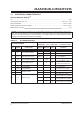
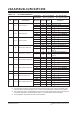
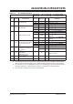
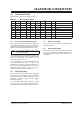
TABLE 2-1: PIN FUNCTION TABLE
Name DFN
(1)
MSOP PDIP SOIC SOIJ TDFN
(1)
TSSOP CSP Function
A0 1 1 1 1 1 1 3 User Configurable Chip Select
A1 2 2 2 2 2 2 2 User Configurable Chip Select
A2 3 3 3 3 3 3 3 5 User Configurable Chip Select
V
SS 4 4 4 4 4 4 4 8 Ground
SDA 5 5 5 5 5 5 5 6 Serial Address/Data I/O
SCL 6 6 6 6 6 6 6 7 Serial Clock
WP 7 7 7 7 7 7 7 4 Write-Protect Input
V
CC 8 8 8 8 8 8 8 1 Power Supply
Note 1: Exposed pad on DFN/TDFN can be connected to V
SS or left floating.
Note: For the MSOP package only, pins A0 and
A1 are not connected.