
Data Sheet

1998-2021 Microchip Technology Inc. DS20001203X-page 5
24AA256/24LC256/24FC256
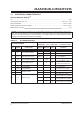
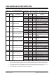
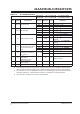
11 TSU:WP WP Setup Time
4000 ns 1.7V
V
CC 2.5V
600 ns 2.5V
VCC 5.5V
600 ns 1.7V
VCC 5.5V (24FC256)
12 T
HD:WP WP Hold Time
4700 ns 1.7V
V
CC 2.5V
1300 ns 2.5V
VCC 5.5V
1300 ns 1.7V
VCC 5.5V (24FC256)
13 T
AA Output Valid from Clock
3500 ns 1.7 V
V
CC 2.5V (Note 2)
900 ns 2.5 V
VCC 5.5V (Note 2)
900 ns
1.7V
VCC 2.5V (24FC256)
(Note 2)
400 ns
2.5 V
VCC 5.5V (24FC256)
(Note 2)
14 T
BUF
Bus Free Time: The time
the bus must be free before
a new transmission can
start
4700 ns 1.7V
V
CC 2.5V
1300 ns 2.5V
VCC 5.5V
1300 ns 1.7V
VCC 2.5V (24FC256)
500 ns 2.5V
VCC 5.5V (24FC256)
15 T
OF
Output fall time from VIH
minimum to VIL maximum
C
B 100 pF
10 + 0.1C
B
250 ns All except 24FC256 (Note 1)
250 ns All except 24FC256 (Note 1)
16 T
SP
Input Filter Spike
Suppression
(SDA and SCL pins)
50 ns
All except 24FC256
(Notes 1 and 3)
17 T
WC
Write Cycle Time
(byte or page)
5ms
18 Endurance 1,000,000 cycles +25°C, 5.5V, Page mode (Note 4)
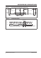
TABLE 1-2: AC CHARACTERISTICS
AC CHARACTERISTICS (Continued)
Industrial (I): V
CC = +1.7V to 5.5V TA = -40°C to +85°C
Extended (E): V
CC = +1.7V to 5.5V TA = -40°C to +125°C
Param.
No.
Symbol Characteristic Minimum Maximum Units Conditions
Note 1: Not 100% tested. C
B = total capacitance of one bus line in pF.
2: As a transmitter, the device must provide an internal minimum delay time to bridge the undefined region
(minimum 300 ns) of the falling edge of SCL to avoid unintended generation of Start or Stop conditions.
3: The combined T
SP and VHYS specifications are due to new Schmitt Trigger inputs, which provide improved
noise spike suppression. This eliminates the need for a T
I specification for standard operation.
4: This parameter is not tested but ensured by characterization.