
Data Sheet

1998-2021 Microchip Technology Inc. DS20001203X-page 3
24AA256/24LC256/24FC256
1.0 ELECTRICAL CHARACTERISTICS
Absolute Maximum Ratings
()
VCC.............................................................................................................................................................................6.5V
All inputs and outputs w.r.t. V
SS ..........................................................................................................-0.6V to VCC +1.0V
Storage temperature ...............................................................................................................................-65°C to +150°C
Ambient temperature with power applied................................................................................................-40°C to +125°C
ESD protection on all pins
4kV
NOTICE: Stresses above those listed under Absolute Maximum Ratings may cause permanent damage to the
device. This is a stress rating only and functional operation of the device at these or any other conditions above those
indicated in the operational listings of this specification is not implied. Exposure to Absolute Maximum Rating
conditions for extended periods may affect device reliability.
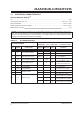
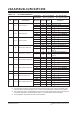
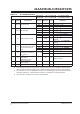
TABLE 1-1: DC CHARACTERISTICS
DC CHARACTERISTICS
Industrial (I): V
CC = +1.7V to 5.5V TA = -40°C to +85°C
Extended (E): V
CC = +1.7V to 5.5V TA = -40°C to +125°C
Param.
No.
Symbol Characteristic Minimum Maximum Units Conditions
D1 V
IH High-Level Input Voltage 0.7 VCC V
D2 V
IL Low-Level Input Voltage
0.3 V
CC VVCC 2.5V
0.2 V
CC VVCC < 2.5V
D3 V
HYS
Hysteresis of Schmitt Trigger
Inputs (SDA, SCL pins)
0.05 V
CC VVCC 2.5V (Note 1)
D4 V
OL Low-Level Output Voltage 0.40 V
I
OL = 3.0 mA @ VCC = 4.5V
I
OL = 2.1 mA @ VCC = 2.5V
D5 I
LI Input Leakage Current ±1 μA
V
IN = VSS or VCC, WP = VSS
VIN = VSS or VCC, WP = VCC
D6 ILO Output Leakage Current ±1 μAVOUT = VSS or VCC
D7
C
IN,
C
OUT
Pin Capacitance
(all inputs/outputs)
10 pF
VCC = 5.0V (Note 1)
T
A = +25°C, FCLK = 1 MHz
D8 I
CC Read
Operating Current
400 μAVCC = 5.5V, SCL = 400 kHz
D9 I
CC Write 3mAVCC = 5.5V
D10 I
CCS Standby Current
1 μA
SDA = SCL = V
CC =3.6V
A0, A1, A2, WP = V
SS, I-Temp.
1.5 μA
SDA = SCL = V
CC =5.5V
A0, A1, A2, WP = V
SS, I-Temp.
5 μA
SDA = SCL = V
CC =5.5V
A0, A1, A2, WP = V
SS, E-Temp.
Note 1: This parameter is periodically sampled and not 100% tested.